MAT02 Datasheet
Low Noise, Matched Dual Monolithic Transistor
Low Noise, Matched Dual Monolithic Transistor
| Part No. | In Stock | Price | Packaging | SPQ | Marking | MSL | Pins | Temp Range | Package Description |
The design of the MAT02 series of NPN dual monolithic transistors is optimized for very low noise, low drift and low rBE. Precision Monolithics’ exclusive Silicon Nitride “TriplePassivation” process stabilizes the critical device parametersover wide ranges of temperature and elapsed time. Also, the high current gain (hFE) of the MAT02 is maintained over a wide range of collector current. Exceptional characteristics of the MAT02 include offset voltage of 50 µV max (A/E grades) and 150 µV max F grade. Device performance is specified over the full military temperature range as well as at 25°C.
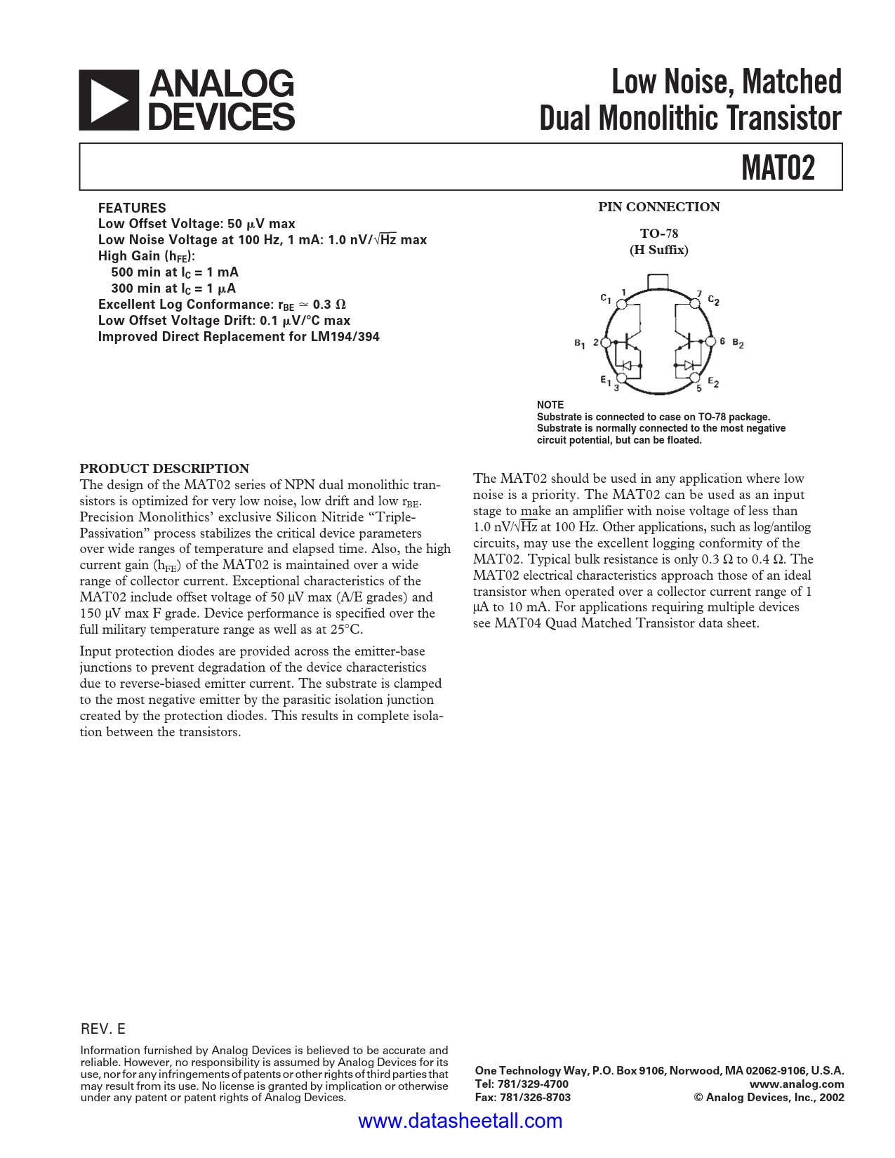
Input protection diodes are provided across the emitter-base junctions to prevent degradation of the device characteristics due to reverse-biased emitter current. The substrate is clamped to the most negative emitter by the parasitic isolation junction created by the protection diodes. This results in complete isolation between the transistors.
The MAT02 should be used in any application where low noise is a priority. The MAT02 can be used as an input stage to make an amplifier with noise voltage of less than 1.0 nV/√Hz at 100 Hz. Other applications, such as log/antilog circuits, may use the excellent logging conformity of the MAT02. Typical bulk resistance is only 0.3 Ω to 0.4 Ω. The MAT02 electrical characteristics approach those of an ideal transistor when operated over a collector current range of 1µA to 10 mA. For applications requiring multiple devices see MAT04 Quad Matched Transistor data sheet.