ADRF5051 Datasheet
Silicon SP4T Switch, Nonreflective, 9kHz to 20GHz
Silicon SP4T Switch, Nonreflective, 9kHz to 20GHz
| Part No. | In Stock | Price | Packaging | SPQ | Marking | MSL | Pins | Temp Range | Package Description |
| ADRF5051BCCZN | 0 | $0 | Reel | 1500 | 1 | 24 | -40°C ~ 105°C | 24-Terminal LGA | |
| ADRF5051BCCZN-R7 | 0 | $0 | Reel | 1500 | 1 | 24 | -40°C ~ 105°C | 24-Terminal LGA |
The ADRF5051 is a nonreflective SP4T switch manufactured in a silicon on insulator (SOI) process.
The ADRF5051 operates from 9kHz to 20GHz with an insertion loss of lower than 1.20dB and an isolation higher than 47dB. The device has RF input power handling capability of 33dBm through path, 18dBm terminated path, and 30dBm hot switching at the RF common (RFC) port.
The ADRF5051 operates with a dual-supply voltage +3.3V and −3.3V. The device can also operate with a single positive supply voltage (VDD) applied while the negative supply pin (VSS) is tied to ground. In this operating condition, the small signal performance is maintained while the switching characteristics, linearity, and power handling performance are derated, see Table 2 in data sheet.
The ADRF5051 employs complimentary metal-oxide semiconductor (CMOS)- and low voltage transistor to transistor logic (LVTTL)-compatible controls.
The device has enable (EN) and logic select (LS) controls. Pulling the EN pin to high activates an all-off state while pulling the LS pin high inverts the throw port selection logic, allowing ease of use for a back-to-back application. See the Theory of Operation section, Table 7 in data sheet, and the Back-to-Back Application section for additional information.
The ADRF5051 is pin compatible with the ADRF5042 and ADRF5043, ADRF5048, ADRF5049, and ADRF5050.
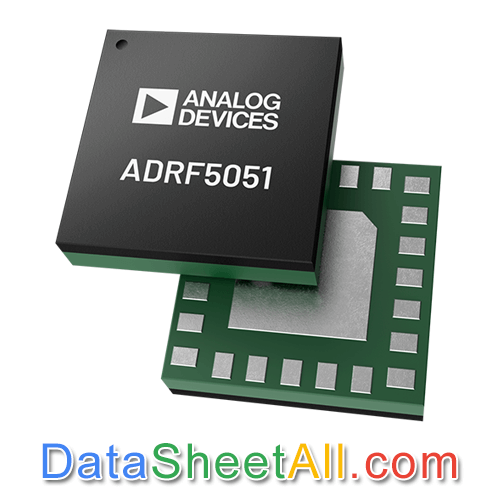
The ADRF5051 comes in a 24-terminal, 3 mm × 3 mm, RoHS compliant, land grid array (LGA) package and can operate from −40°C to +105°C.