ADP5056 Datasheet
Triple Buck Regulator Integrated Power Solution
Triple Buck Regulator Integrated Power Solution
| Part No. | In Stock | Price | Packaging | SPQ | Marking | MSL | Pins | Temp Range | Package Description |
| ADP5056ACCZ-R7 | 1500pcs | $5.004 | Reel | 1500 | ADP5056 | 3 | 43 | -40°C ~ 150°C | 43-Terminal LGA |
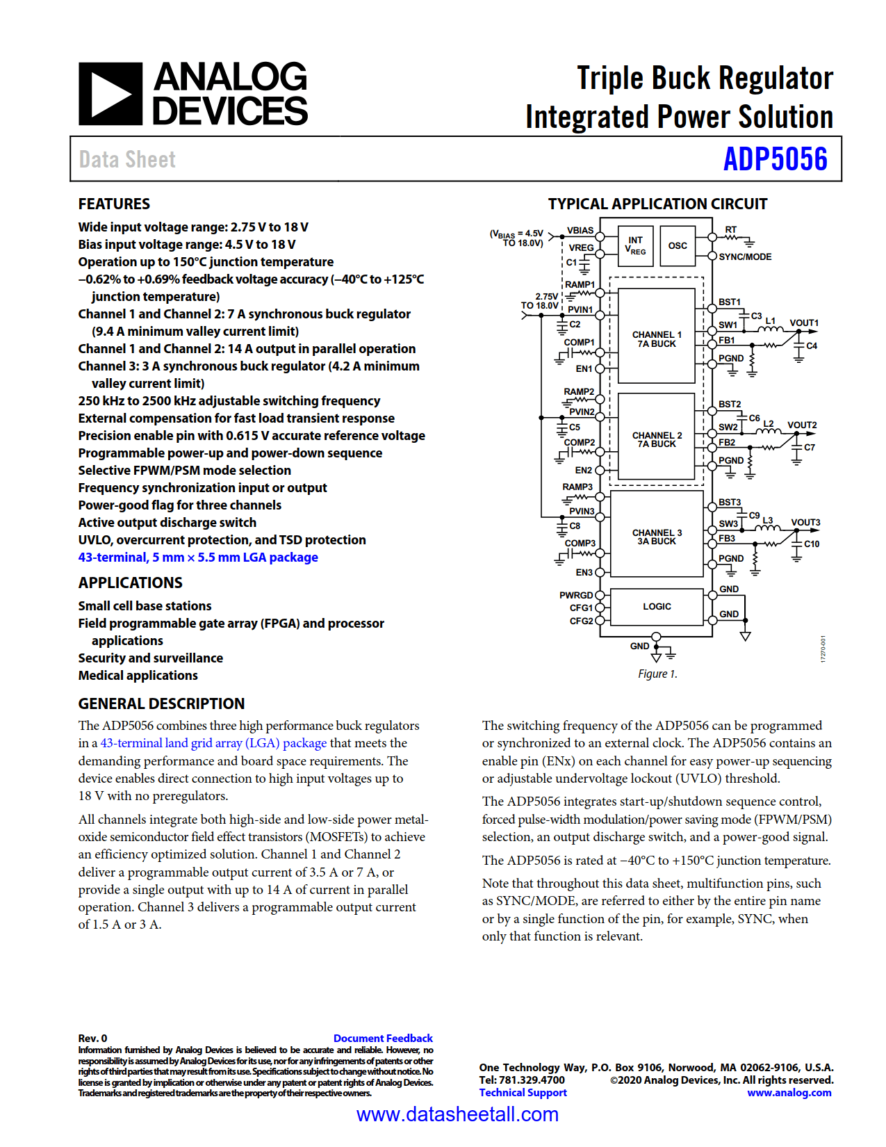
The ADP5056 combines three high performance buck regulators in a 43-terminal land grid array (LGA) package that meets the demanding performance and board space requirements. The device enables direct connection to high input voltages up to 18 V with no preregulators.
All channels integrate both high-side and low-side power metaloxide semiconductor field effect transistors (MOSFETs) to achieve an efficiency optimized solution. Channel 1 and Channel 2 deliver a programmable output current of 3.5 A or 7 A, or provide a single output with up to 14 A of current in parallel operation. Channel 3 delivers a programmable output current of 1.5 A or 3 A.
The switching frequency of the ADP5056 can be programmed or synchronized to an external clock. The ADP5056 contains an enable pin (ENx) on each channel for easy power-up sequencing or adjustable undervoltage lockout (UVLO) threshold.
The ADP5056 integrates start-up/shutdown sequence control, forced pulse-width modulation/power saving mode (FPWM/PSM) selection, an output discharge switch, and a power-good signal.
The ADP5056 is rated at −40°C to +150°C junction temperature.
Note that throughout this data sheet, multifunction pins, such as SYNC/MODE, are referred to either by the entire pin name or by a single function of the pin, for example, SYNC, when only that function is relevant.