ADP5052 Datasheet
5-Channel Integrated Power Solution with Quad Buck Regulators and 200 mA LDO Regulator
5-Channel Integrated Power Solution with Quad Buck Regulators and 200 mA LDO Regulator
| Part No. | In Stock | Price | Packaging | SPQ | Marking | MSL | Pins | Temp Range | Package Description |
| ADP5052ACPZ-R7 | 3750pcs | $5.472 | Reel | 750 | ADP5052ACPZ | 3 | 48 | -40°C ~ 125°C | 48-Lead LFCSP |
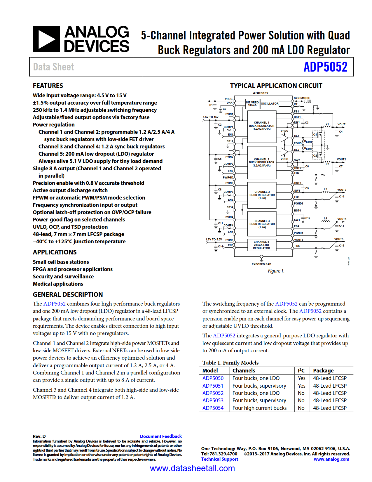
The ADP5052 combines four high performance buck regulators and one 200 mA low dropout (LDO) regulator in a 48-lead LFCSP package that meets demanding performance and board space requirements. The device enables direct connection to high input voltages up to 15 V with no preregulators.
Channel 1 and Channel 2 integrate high-side power MOSFETs and low-side MOSFET drivers. External NFETs can be used in low-side power devices to achieve an efficiency optimized solution and deliver a programmable output current of 1.2 A, 2.5 A, or 4 A. Combining Channel 1 and Channel 2 in a parallel configuration can provide a single output with up to 8 A of current.
Channel 3 and Channel 4 integrate both high-side and low-side MOSFETs to deliver output current of 1.2 A.
The switching frequency of the ADP5052 can be programmed or synchronized to an external clock. The ADP5052 contains a precision enable pin on each channel for easy power-up sequencing or adjustable UVLO threshold.
The ADP5052 integrates a general-purpose LDO regulator with low quiescent current and low dropout voltage that provides up to 200 mA of output current.