ADP5051 Datasheet
Integrated Power Solution with Quad Buck Regulators, Supervisory, and I2C Interface
Integrated Power Solution with Quad Buck Regulators, Supervisory, and I2C Interface
| Part No. | In Stock | Price | Packaging | SPQ | Marking | MSL | Pins | Temp Range | Package Description |
| ADP5051ACPZ-R7 | 500pcs | $5.814 | Reel | 750 | ADP5051ACPZ | 3 | 48 | -40°C ~ 125°C | 48-Lead LFCSP |
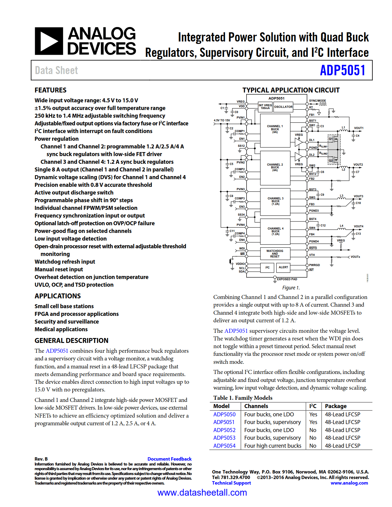
The ADP5051 combines four high performance buck regulators, and a supervisory circuit with a voltage monitor, watchdog, and manual reset in a 48-lead LFCSP package that meets demanding performance and board space requirements. The device enables direct connection to high input voltages up to 15.0 V with no preregulators.
Channel 1 and Channel 2 integrate high-side power MOSFET and low-side MOSFET drivers. In low-side power devices, use external NFETs to achieve an efficiency optimized solution and deliver a programmable output current of 1.2 A, 2.5 A, or 4 A.
Combining Channel 1 and Channel 2 in a parallel configuration provides a single output with up to 8 A of current. Channel 3 and Channel 4 integrate both high-side and low-side MOSFETs to deliver an output current of 1.2 A.
The ADP5051 supervisory circuits monitor voltage level. The watchdog timer generates a reset when the WDI does not toggle within a preset timeout period. Select manual reset functionality via the processor reset mode or system power on/off switch mode.
The optional I2C interface offers flexible configurations, including adjustable and fixed output voltage, junction temperature overheat warning, low input voltage detection, and dynamic voltage scaling.