ADL5309 Datasheet
Dual, 188 dB Range, 10 pA to 25 mA, Logarithmic Converter
Dual, 188 dB Range, 10 pA to 25 mA, Logarithmic Converter
| Part No. | In Stock | Price | Packaging | SPQ | Marking | MSL | Pins | Temp Range | Package Description |
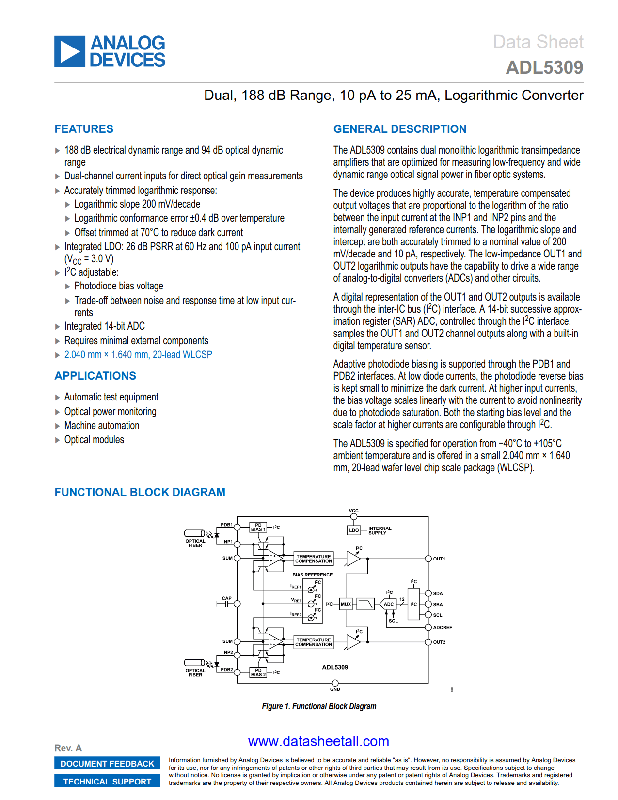
The ADL5309 contains dual monolithic logarithmic transimpedance amplifiers that are optimized for measuring low-frequency and wide dynamic range optical signal power in fiber optic systems.
The device produces highly accurate, temperature compensated output voltages that are proportional to the logarithm of the ratio between the input current at the INP1 and INP2 pins and the internally generated reference currents. The logarithmic slope and intercept are both accurately trimmed to a nominal value of 200 mV/decade and 10 pA, respectively. The low-impedance OUT1 and OUT2 logarithmic outputs have the capability to drive a wide range of analog-to-digital converters (ADCs) and other circuits.
A digital representation of the OUT1 and OUT2 outputs is available through the inter-IC bus (I2C) interface. A 14-bit successive approximation register (SAR) ADC, controlled through the I2C interface, samples the OUT1 and OUT2 channel outputs along with a built-in digital temperature sensor.
Adaptive photodiode biasing is supported through the PDB1 and PDB2 interfaces. At low diode currents, the photodiode reverse bias is kept small to minimize the dark current. At higher input currents, the bias voltage scales linearly with the current to avoid nonlinearity due to photodiode saturation. Both the starting bias level and the scale factor at higher currents are configurable through I2C.
The ADL5309 is specified for operation from −40°C to +105°C ambient temperature and is offered in a small 2.040 mm × 1.640 mm, 20-lead wafer level chip scale package (WLCSP).