ADF4401A Datasheet
Translation Loop, PLL, VCO Module
Translation Loop, PLL, VCO Module
| Part No. | In Stock | Price | Packaging | SPQ | Marking | MSL | Pins | Temp Range | Package Description |
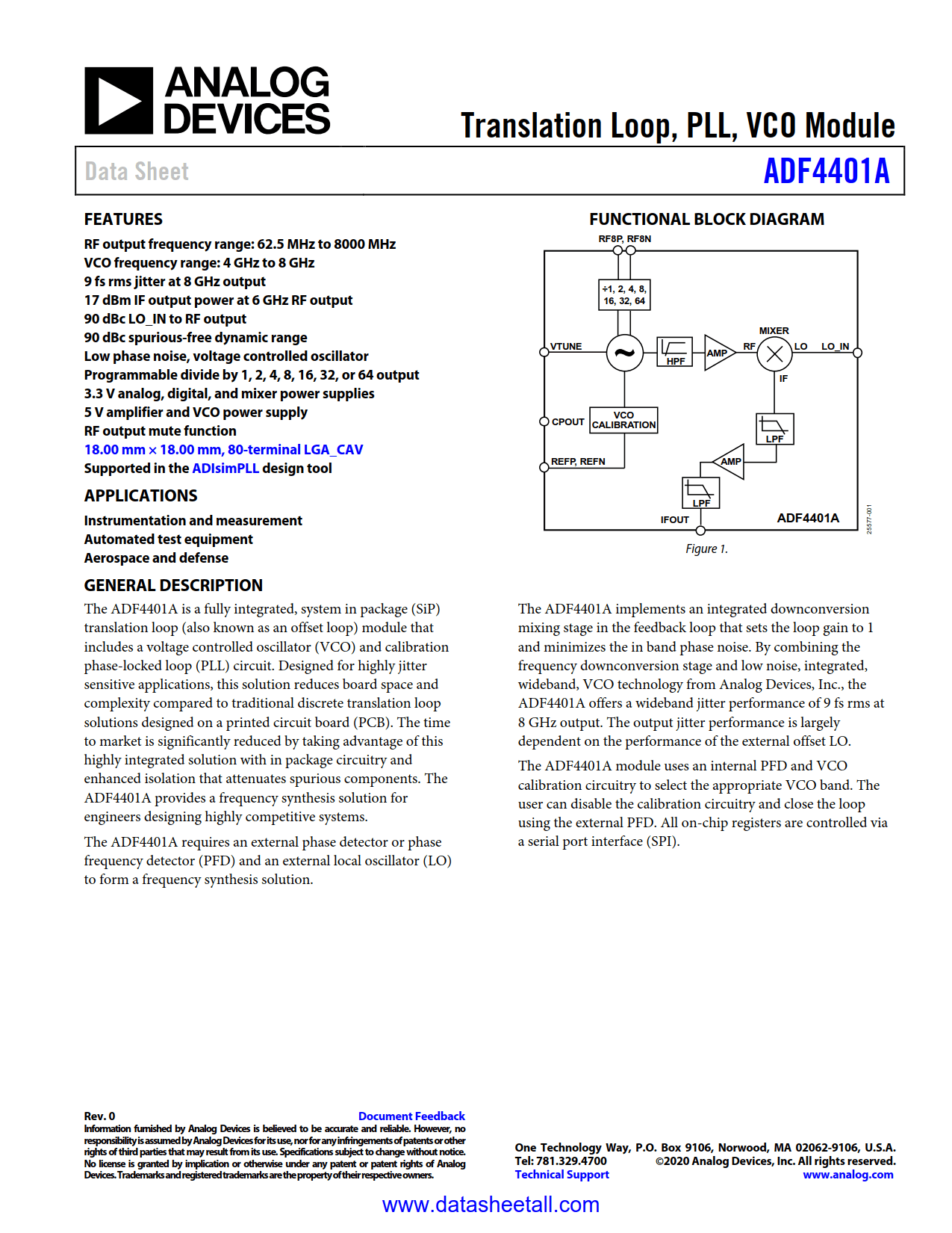
The ADF4401A is a fully integrated, system in package (SiP) translation loop (also known as an offset loop) module that includes a voltage controlled oscillator (VCO) and calibration phase-locked loop (PLL) circuit. Designed for highly jitter sensitive applications, this solution reduces board space and complexity compared to traditional discrete translation loop solutions designed on a printed circuit board (PCB). The time to market is significantly reduced by taking advantage of this highly integrated solution with in package circuitry and enhanced isolation that attenuates spurious components. The ADF4401A provides a frequency synthesis solution for engineers designing highly competitive systems.
The ADF4401A requires an external phase detector or phase frequency detector (PFD) and an external local oscillator (LO) to form a frequency synthesis solution.
The ADF4401A implements an integrated downconversion mixing stage in the feedback loop that sets the loop gain to 1 and minimizes the in band phase noise. By combining the frequency downconversion stage and low noise, integrated, wideband, VCO technology from Analog Devices, Inc., the ADF4401A offers a wideband jitter performance of 9 fs rms at 8 GHz output. The output jitter performance is largely dependent on the performance of the external offset LO.
The ADF4401A module uses an internal PFD and VCO calibration circuitry to select the appropriate VCO band. The user can disable the calibration circuitry and close the loop using the external PFD. All on-chip registers are controlled via a serial port interface (SPI).