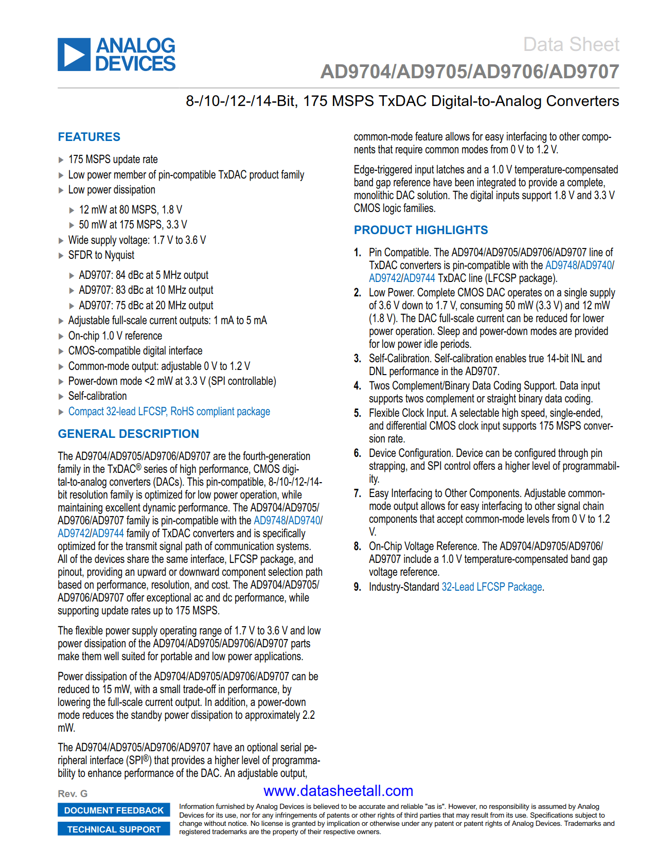
AD9706 Datasheet

12-Bit, 175 MSPS TxDAC Digital-to-Analog Converter

Part No.:
AD9706
Manufacturer:
Analog Devices, Inc.
Page:
43 Pages
Size:
2778 KB
Views:
0
Update Time:
2026-02-05 16:44:18

AD9706 DataSheet Applicable Part

Part No. In Stock Price Packaging SPQ Marking MSL Pins Temp Range Package Description
SPQ:Standard Pack Quantity;MSL:Moisture Sensitivity Level

AD9706 DataSheet PDF

AD9706 Features

  • 175 MSPS update rate
  • Low power member of pin-compatible TxDAC product family
  • Low power dissipation
    • 12 mW at 80 MSPS, 1.8 V
    • 50 mW at 175 MSPS, 3.3 V
  • Wide supply voltage: 1.7 V to 3.6 V
  • Adjustable full-scale current outputs: 1 mA to 5 mA
  • On-chip 1.0 V reference
  • CMOS-compatible digital interface
  • Common-mode output: adjustable 0 V to 1.2 V
  • Power-down mode <2 mW at 3.3 V (SPI controllable)
  • Self-calibration
  • Compact 32-lead LFCSP, RoHS compliant package

AD9706 Description

The AD9706 are the fourth-generation family in the TxDAC series of high performance, CMOS digital-to-analog converters (DACs). This pin-compatible, 12-bit resolution family is optimized for low power operation, while maintaining excellent dynamic performance. The AD9706 is pin-compatible with the AD9748/AD9740/AD9742/AD9744 family of TxDAC converters and is specifically optimized for the transmit signal path of communication systems. All of the devices share the same interface, LFCSP package, and pinout, providing an upward or downward component selection path based on performance, resolution, and cost. The AD9706 offers exceptional ac and dc performance, while supporting update rates up to 175 MSPS.

The flexible power supply operating range of 1.7 V to 3.6 V and low power dissipation of the AD9706 parts make them well suited for portable and low power applications.

Power dissipation of the AD9706 can be reduced to 15 mW, with a small trade-off in performance, by lowering the full-scale current output. In addition, a power-down mode reduces the standby power dissipation to approximately 2.2 mW.

The AD9706 has an optional serial peripheral interface (SPI®) that provides a higher level of programmability to enhance performance of the DAC. An adjustable output, common-mode feature allows for easy interfacing to other components that require common modes from 0 V to 1.2 V.

Edge-triggered input latches and a 1.0 V temperature-compensated band gap reference have been integrated to provide a complete, monolithic DAC solution. The digital inputs support 1.8 V and 3.3 V CMOS logic families.

PRODUCT HIGHLIGHTS

  1. Pin Compatible. The AD9706 line of TxDAC converters is pin-compatible with the AD9748/AD9740/AD9742/AD9744 TxDAC line (LFCSP package).
  2. Low Power. Complete CMOS DAC operates on a single supply of 3.6 V down to 1.7 V, consuming 50 mW (3.3 V) and 12 mW (1.8 V). The DAC full-scale current can be reduced for lower power operation. Sleep and power-down modes are provided for low power idle periods.
  3. Self-Calibration.
  4. Twos Complement/Binary Data Coding Support. Data input supports twos complement or straight binary data coding.
  5. Flexible Clock Input. A selectable high speed, single-ended,and differential CMOS clock input supports 175 MSPS conversion rate.
  6. Device Configuration. Device can be configured through pin strapping, and SPI control offers a higher level of programmability.
  7. Easy Interfacing to Other Components. Adjustable common-mode output allows for easy interfacing to other signal chain components that accept common-mode levels from 0 V to 1.2 V.
  8. On-Chip Voltage Reference. The AD9706 include a 1.0 V temperature-compensated band gap voltage reference.
  9. Industry-Standard 32-Lead LFCSP Package.

AD9706 Datasheet FAQs