AD9634 Datasheet

12-Bit, 170 MSPS/210 MSPS/250 MSPS, 1.8 V Analog-to-Digital Converter

Part No.:
AD9634
Manufacturer:
Analog Devices, Inc.
Page:
30 Pages
Size:
1489 KB
Views:
0
Update Time:
2025-09-22 15:44:42

AD9634 DataSheet Applicable Part

Part No. In Stock Price Packaging SPQ Marking MSL Pins Temp Range Package Description
SPQ:Standard Pack Quantity;MSL:Moisture Sensitivity Level

AD9634 DataSheet PDF

AD9634 Features

  • SNR = 69.7 dBFS at 185 MHz AIN and 250 MSPS
  • SFDR = 87 dBc at 185 MHz AIN and 250 MSPS
  • −150.6 dBFS/Hz input noise at 185 MHz, −1 dBFS AIN and 250 MSPS
  • Total Power consumption: 360 @ 250 MSPS
  • 1.8 V supply voltages
  • LVDS (ANSI-644 levels) outputs
  • Integer 1-to-8 input clock divider (625 MHz maximum input)
  • Sample rates of up to 250 MSPS
  • IF sampling frequencies of up to 350 MHz
  • Internal ADC voltage reference
  • Flexible analog input range 1.4 V p-p to 2.0 V p-p (1.75 V p-p nominal)
  • See data sheet for additional features

AD9634 Applications

  • Communications
  • Diversity radio systems
  • Multimode digital receivers (3G)
    TD-SCDMA, WiMax, WCDMA, CDMA2000, GSM, EDGE, LTE
  • I/Q demodulation systems
  • Smart antenna systems
  • General-purpose software radios
  • Ultrasound equipment
  • Broadband data applications

AD9634 Description

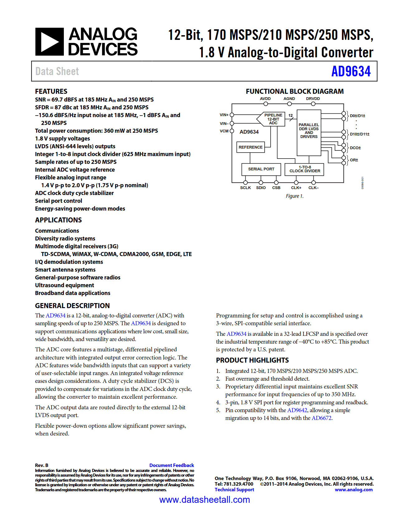
The AD9634 is a 12-bit, analog-to-digital converter (ADC) with sampling speeds of up to 250 MSPS. The AD9634 is designed to support communications applications where low cost, small size, wide bandwidth, and versatility are desired.

The ADC core features a multistage, differential pipelined architecture with integrated output error correction logic. The ADC features wide bandwidth inputs that can support a variety of user-selectable input ranges. An integrated voltage reference eases design considerations. A duty cycle stabilizer (DCS) is provided to compensate for variations in the ADC clock duty cycle, allowing the converter to maintain excellent performance.

The ADC output data are routed directly to the external 12-bit LVDS output port.

Flexible power-down options allow significant power savings, when desired.

Programming for setup and control is accomplished using a 3-wire, SPI-compatible serial interface.

The AD9634 is available in a 32-lead LFCSP and is specified over the industrial temperature range of −40°C to +85°C. This product is protected by a U.S. patent.

PRODUCT HIGHLIGHTS

  1. Integrated 12-bit, 170 MSPS/210 MSPS/250 MSPS ADC.
  2. Fast overrange and threshold detect.
  3. Proprietary differential input maintains excellent SNR performance for input frequencies up to 350 MHz.
  4. 3-pin, 1.8V SPI port for register programming and readback.
  5. Pin compatibility with the AD9642, allowing a simple migration up to 14 bits, and with the AD6672.

AD9634 Datasheet FAQs