AD6672 Datasheet
IF Receiver
IF Receiver
| Part No. | In Stock | Price | Packaging | SPQ | Marking | MSL | Pins | Temp Range | Package Description |
The AD6672 is an 11-bit intermediate receiver with sampling speeds of up to 250 MSPS. The AD6672 is designed to support communications applications, where low cost, small size, wide bandwidth, and versatility are desired.
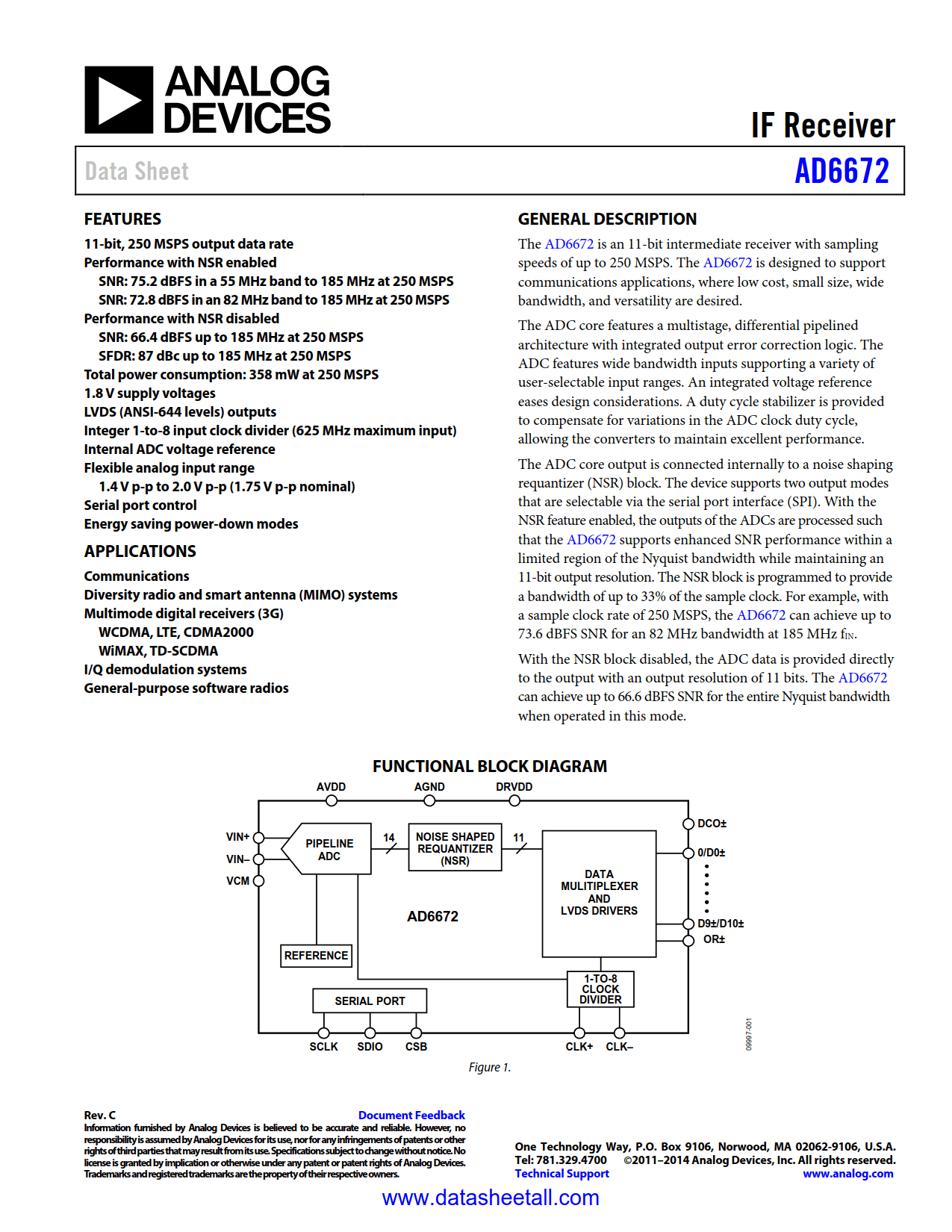
The ADC core features a multistage, differential pipelined architecture with integrated output error correction logic. The ADC features wide bandwidth inputs supporting a variety of user-selectable input ranges. An integrated voltage reference eases design considerations. A duty cycle stabilizer is provided to compensate for variations in the ADC clock duty cycle, allowing the converters to maintain excellent performance.
The ADC core output is connected internally to a noise shaping requantizer (NSR) block. The device supports two output modes that are selectable via the serial port interface (SPI). With the NSR feature enabled, the outputs of the ADCs are processed such that the AD6672 supports enhanced SNR performance within a limited region of the Nyquist bandwidth while maintaining an 11-bit output resolution. The NSR block is programmed to provide a bandwidth of up to 33% of the sample clock. For example, with a sample clock rate of 250 MSPS, the AD6672 can achieve up to 73.6 dBFS SNR for an 82 MHz bandwidth at 185 MHz fIN.
With the NSR block disabled, the ADC data is provided directly to the output with an output resolution of 11 bits. The AD6672 can achieve up to 66.6 dBFS SNR for the entire Nyquist bandwidth when operated in this mode.