AD5689R-EP Datasheet
Dual, 16-Bit nanoDAC+ with 4 ppm/°C Reference, SPI Interface
Dual, 16-Bit nanoDAC+ with 4 ppm/°C Reference, SPI Interface
| Part No. | In Stock | Price | Packaging | SPQ | Marking | MSL | Pins | Temp Range | Package Description |
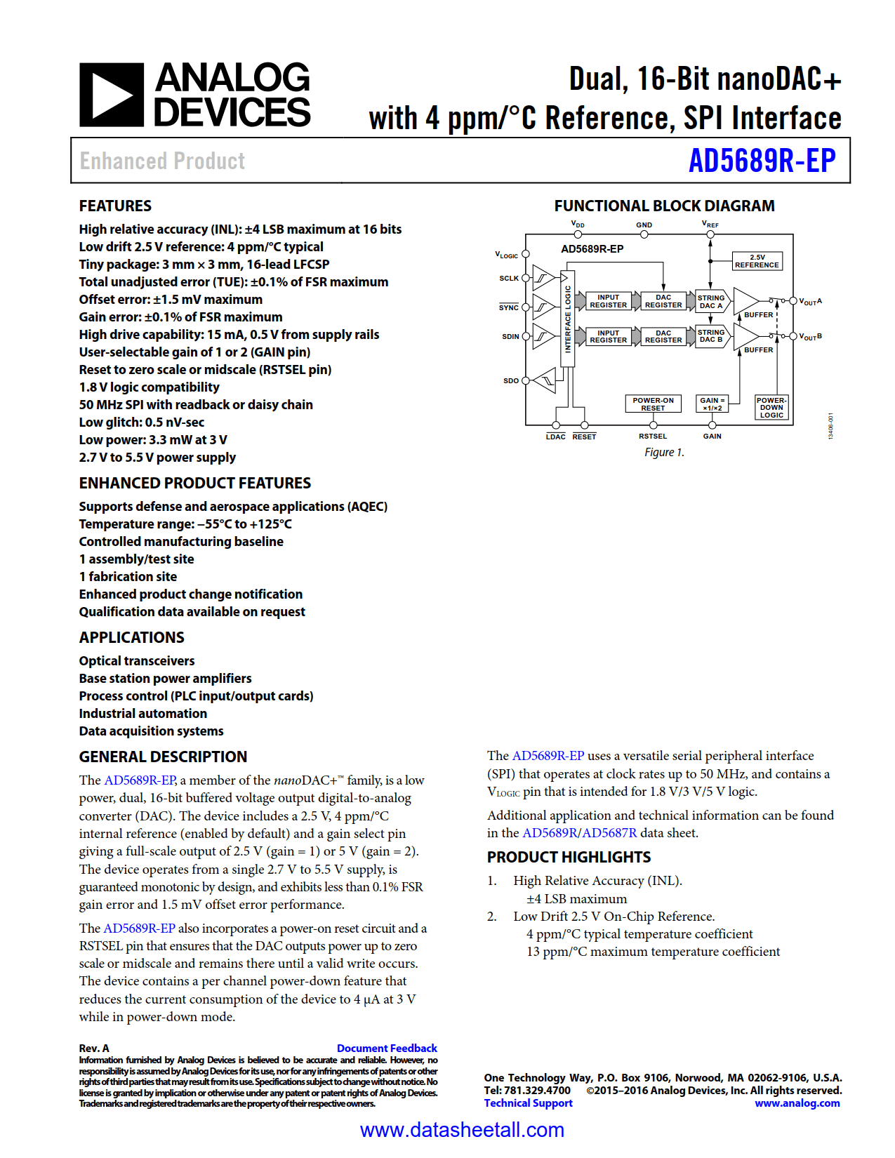
The AD5689R-EP, a member of the nanoDAC+™ family, is a low power, dual, 16-bit buffered voltage output digital-to-analog converter (DAC). The device includes a 2.5 V, 4 ppm/°C internal reference (enabled by default) and a gain select pin giving a full-scale output of 2.5 V (gain = 1) or 5 V (gain = 2). The device operates from a single 2.7 V to 5.5 V supply, is guaranteed monotonic by design, and exhibits less than 0.1% FSR gain error and 1.5 mV offset error performance.
The AD5689R-EP also incorporates a power-on reset circuit and a RSTSEL pin that ensures that the DAC outputs power up to zero scale or midscale and remains there until a valid write occurs. The device contains a per channel power-down feature that reduces the current consumption of the device to 4 μA at 3 V while in power-down mode.
The AD5689R-EP uses a versatile serial peripheral interface (SPI) that operates at clock rates up to 50 MHz, and contains a VLOGIC pin that is intended for 1.8 V/3 V/5 V logic.
Additional application and technical information can be found in the AD5689R data sheet.
PRODUCT HIGHLIGHTS
1. High Relative Accuracy (INL).
±4 LSB maximum
2. Low Drift 2.5 V On-Chip Reference.
4 ppm/°C typical temperature coefficient
13 ppm/°C maximum temperature coefficient