AD4630-24 Datasheet
24-Bit, 2 MSPS Dual Channel SAR ADC
24-Bit, 2 MSPS Dual Channel SAR ADC
| Part No. | In Stock | Price | Packaging | SPQ | Marking | MSL | Pins | Temp Range | Package Description |
| AD4630-24BBCZ | 260pcs | $37.26 | Tray | 260 | AD4630-24BBCZ | 4 | 64 | -40°C ~ 125°C | 64-Lead BGA |
| AD4630-24BBCZ-RL | 200pcs | $37.26 | Reel | 2000 | AD4630-24BBCZ | 4 | 64 | -40°C ~ 125°C | 64-Lead BGA |
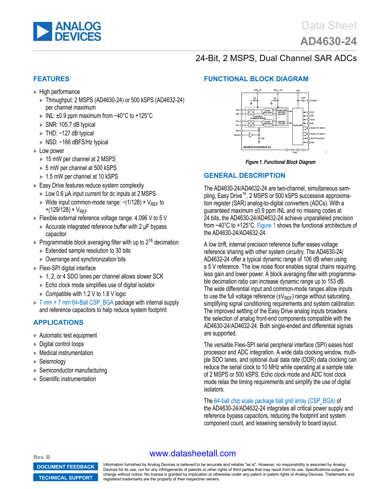
The AD4630-24 are two-channel, simultaneous sampling, Easy Drive™, 2 MSPS successive approximation register (SAR) analog-to-digital converters (ADCs). With a guaranteed maximum ±0.9 ppm INL and no missing codes at 24 bits, the AD4630-24 achieve unparalleled precision from −40°C to +125°C. Figure 1 in the data sheet shows the functional architecture of the AD4630-24.
A low drift, internal precision reference buffer eases voltage reference sharing with other system circuitry. The AD4630-24 offer a typical dynamic range of 106 dB when using a 5 V reference. The low noise floor enables signal chains requiring less gain and lower power. A block averaging filter with programmable decimation ratio can increase dynamic range up to 153 dB. The wide differential input and common-mode ranges allow inputs to use the full voltage reference (±VREF) range without saturating, simplifying signal conditioning requirements and system calibration. The improved settling of the Easy Drive analog inputs broadens the selection of analog front-end components compatible with the AD4630-24. Both single-ended and differential signals are supported.
The versatile Flexi-SPI serial peripheral interface (SPI) eases host processor and ADC integration. A wide data clocking window, multiple SDO lanes, and optional dual data rate (DDR) data clocking can reduce the serial clock to 10 MHz while operating at a sample rate of 2 MSPS or 500 kSPS. Echo clock mode and ADC host clock mode relax the timing requirements and simplify the use of digital isolators.
The 64-ball chip scale package ball grid array (CSP_BGA) of the AD4630-24 integrates all critical power supply and reference bypass capacitors, reducing the footprint and system component count, and lessening sensitivity to board layout.