LTC7891 Datasheet
100 V, Low IQ, Synchronous Step-Down Controller for GaN FETs
100 V, Low IQ, Synchronous Step-Down Controller for GaN FETs
| Part No. | In Stock | Price | Packaging | SPQ | Marking | MSL | Pins | Temp Range | Package Description |
The LTC7891 is a high performance, step-down, dc-to-dc switching regulator controller that drives all N-channel synchronous gallium nitride (GaN) field effect transistor (FET) power stages from input voltages up to 100 V. The LTC7891 solves many of the challenges traditionally faced when using GaN FETs. The LTC7891 simplifies the application design while requiring no protection diodes and no other additional external components compared to a silicon metal-oxide semiconductor field effect transistor (MOSFET) solution.
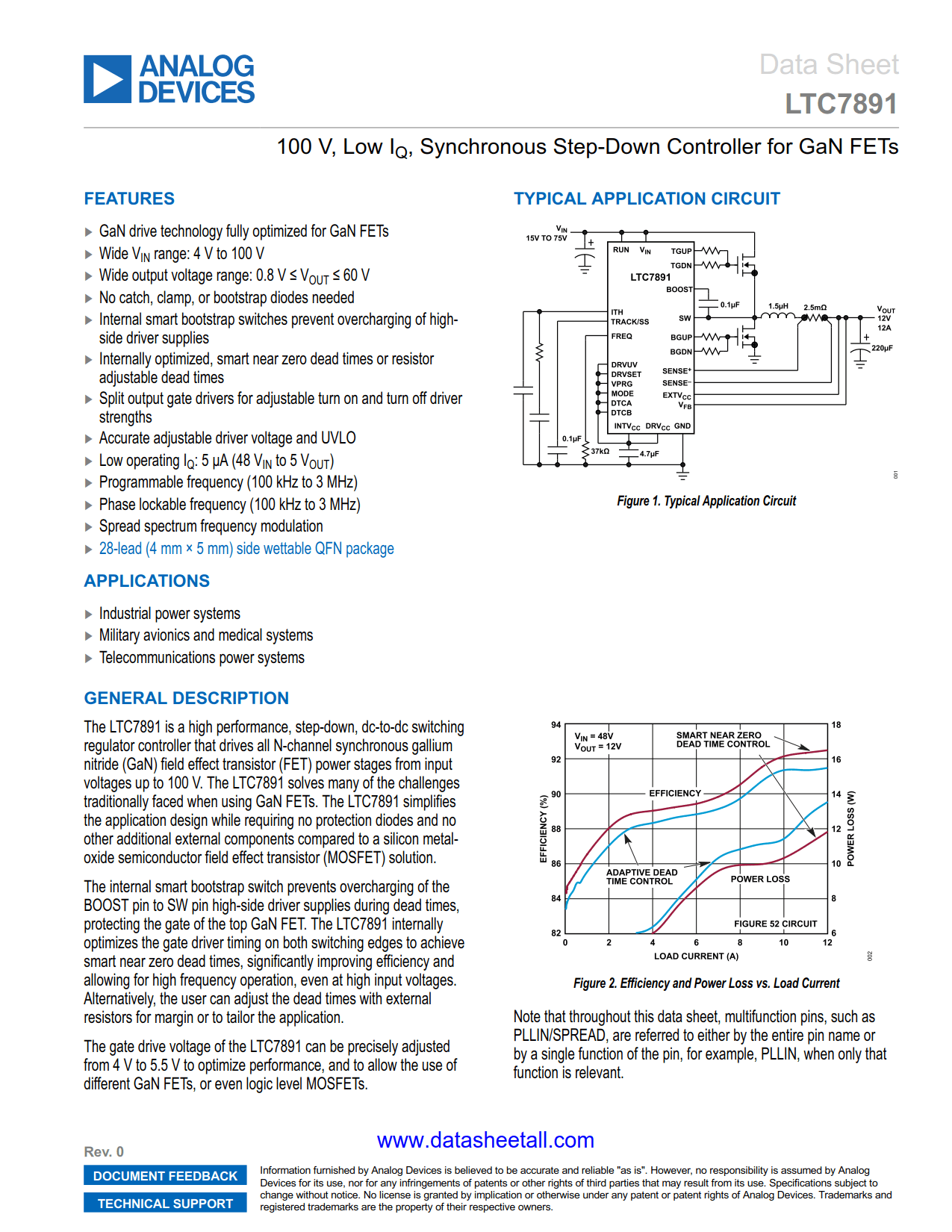
The internal smart bootstrap switch prevents overcharging of the BOOST pin to SW pin high-side driver supplies during dead times, protecting the gate of the top GaN FET. The LTC7891 internally optimizes the gate driver timing on both switching edges to achieve smart near zero dead times, significantly improving efficiency and allowing for high frequency operation, even at high input voltages. Alternatively, the user can adjust the dead times with external resistors for margin or to tailor the application.
The gate drive voltage of the LTC7891 can be precisely adjusted from 4 V to 5.5 V to optimize performance, and to allow the use of different GaN FETs, or even logic level MOSFETs.
Note that throughout this data sheet, multifunction pins, such as PLLIN/SPREAD, are referred to either by the entire pin name or by a single function of the pin, for example, PLLIN, when only that function is relevant.