LTC6957-2 Datasheet
Low Phase Noise, Dual Output Buffer/Driver/Logic Converter
Low Phase Noise, Dual Output Buffer/Driver/Logic Converter
| Part No. | In Stock | Price | Packaging | SPQ | Marking | MSL | Pins | Temp Range | Package Description |
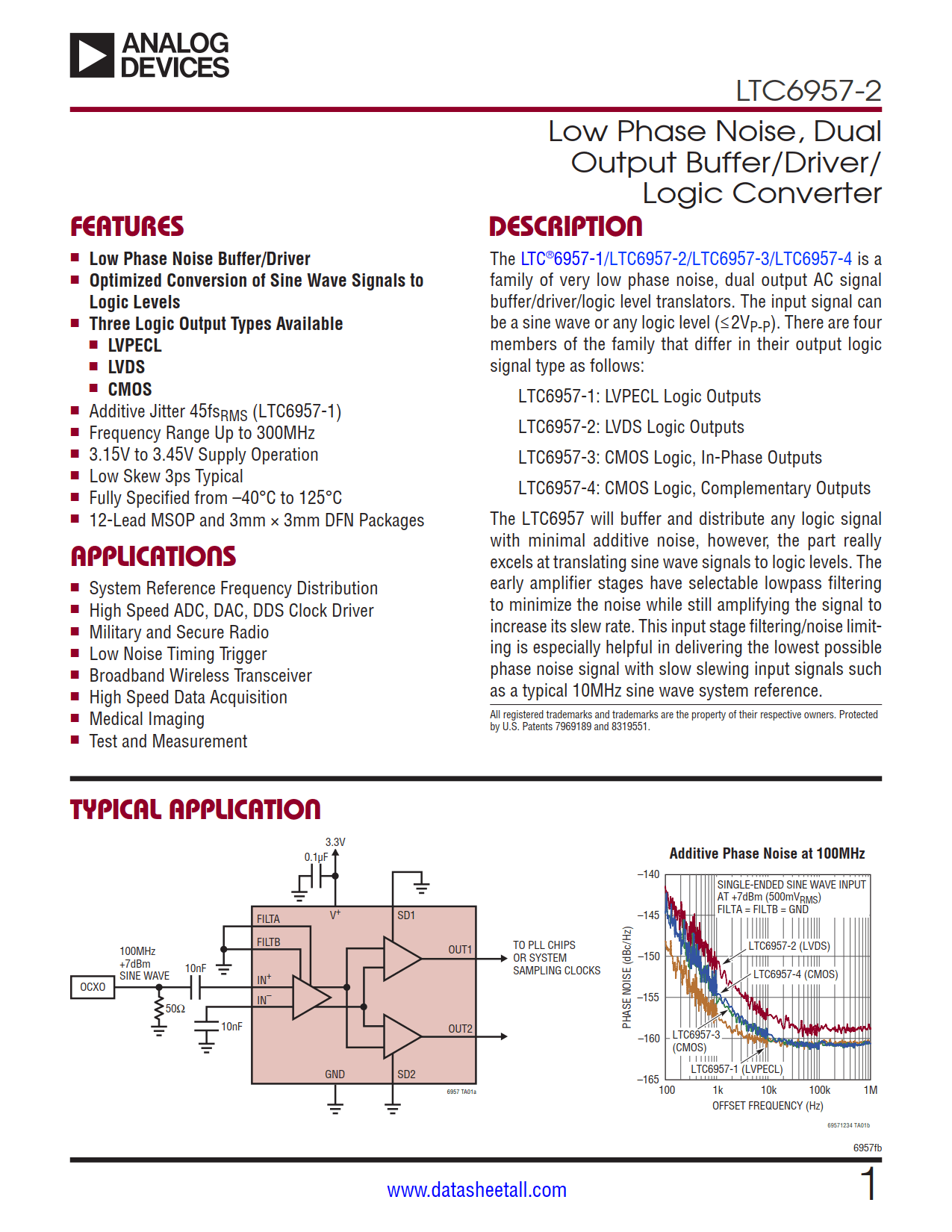
The LTC6957-2 is a family of very low phase noise, dual output AC signal buffer/driver/logic level translators. The input signal can be a sine wave or any logic level (≤2VP-P). There are four members of the family that differ in their output logic signal type as follows:
LTC6957-2: LVDS Logic Outputs
The LTC6957-2 will buffer and distribute any logic signal with minimal additive noise, however, the part really excels at translating sine wave signals to logic levels. The early amplifier stages have selectable lowpass filtering to minimize the noise while still amplifying the signal to increase its slew rate. This input stage filtering/noise limiting is especially helpful in delivering the lowest possible phase noise signal with slow slewing input signals such as a typical 10MHz sine wave system reference.