LTC6269 Datasheet
Dual 500MHz Ultra-Low Bias Current FET Input Op Amp
Dual 500MHz Ultra-Low Bias Current FET Input Op Amp
| Part No. | In Stock | Price | Packaging | SPQ | Marking | MSL | Pins | Temp Range | Package Description |
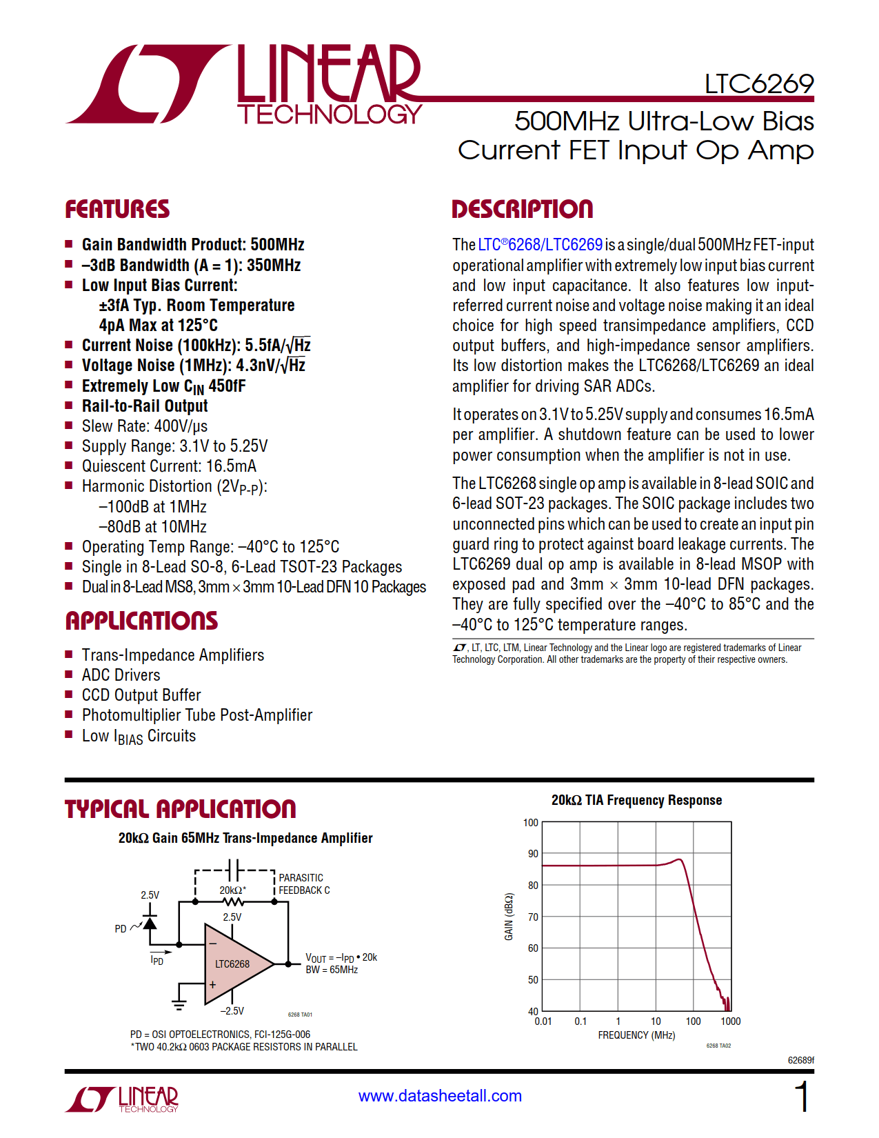
The LTC6269 is a dual 500MHz FET-input operational amplifier with extremely low input bias current and low input capacitance. It also features low input-referred current noise and voltage noise making it an ideal choice for high speed transimpedance amplifiers, CCD output buffers, and high-impedance sensor amplifiers. Its low distortion makes the LTC6269 an ideal amplifier for driving SAR ADCs.
It operates on 3.1V to 5.25V supply and consumes 16.5mA per amplifier. A shutdown feature can be used to lower power consumption when the amplifier is not in use.
The LTC6269 dual op amp is available in 8-lead MSOP with exposed pad and 3mm × 3mm 10-lead DFN packages. The LTC6269 is fully specified over the –40°C to 85°C and the –40°C to 125°C temperature ranges.