LTC2672 Datasheet
Five-Channel, Current Output DAC with Internal Reference and SPI
Five-Channel, Current Output DAC with Internal Reference and SPI
| Part No. | In Stock | Price | Packaging | SPQ | Marking | MSL | Pins | Temp Range | Package Description |
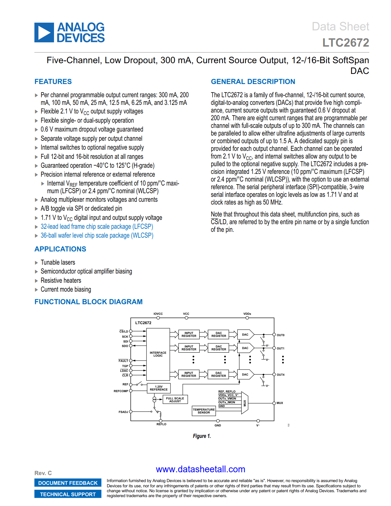
The LTC2672 is a family of five-channel, 12-/16-bit current source, digital-to-analog converters (DACs) that provide five high compliance, current source outputs with guaranteed 0.6 V dropout at 200 mA. There are eight current ranges that are programmable per channel with full-scale outputs of up to 300 mA. The channels can be paralleled to allow either ultrafine adjustments of large currents or combined outputs of up to 1.5 A. A dedicated supply pin is provided for each output channel. Each channel can be operated from 2.1 V to VCC, and internal switches allow any output to be pulled to the optional negative supply. The LTC2672 includes a precision integrated 1.25 V reference (10 ppm/°C maximum (LFCSP) or 2.4 ppm/°C nominal (WLCSP)), with the option to use an external reference. The serial peripheral interface (SPI)-compatible, 3‑wire serial interface operates on logic levels as low as 1.71 V and at clock rates as high as 50 MHz.
Note that throughout this data sheet, multifunction pins, such as CS/LD, are referred to by the entire pin name or by a single function of the pin.