LTC2606 Datasheet
16-Bit Rail-to-Rail DACs with I2C Interface
16-Bit Rail-to-Rail DACs with I2C Interface
| Part No. | In Stock | Price | Packaging | SPQ | Marking | MSL | Pins | Temp Range | Package Description |
The LTC2606 are single 16-bit, 2.7V-to-5.5V rail-to-rail voltage output DACs in a 10-lead DFN package. They have built-in high performance output buffers and are guaranteed monotonic.
These parts establish new board-density benchmarks for 16- and 14-bit DACs and advance performance standards for output drive and load regulation in single-supply, voltage-output DACs.
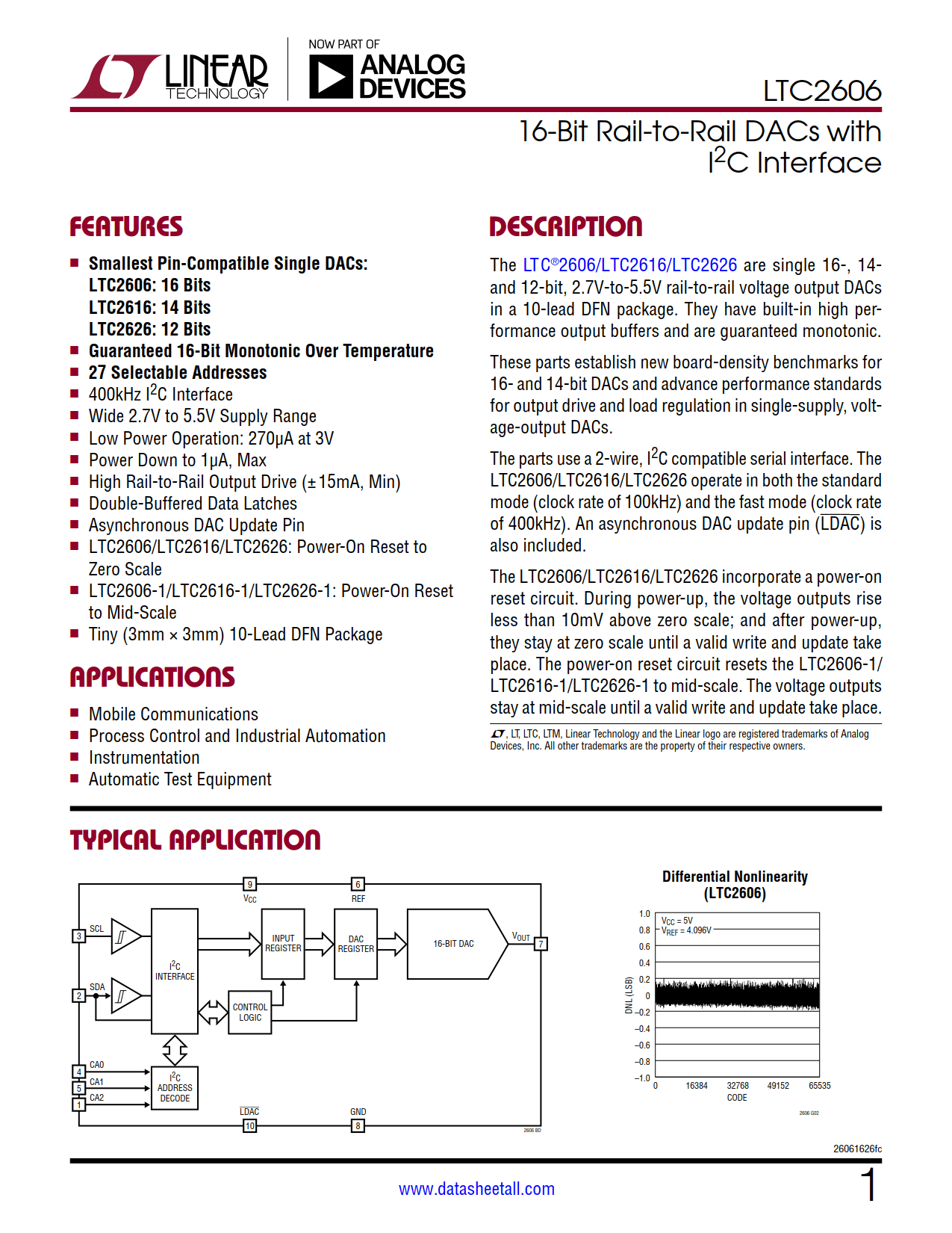
The parts use a 2-wire, I2C compatible serial interface. The LTC2606 operate in both the standard mode (clock rate of 100kHz) and the fast mode (clock rate of 400kHz). An asynchronous DAC update pin (LDAC) is also included.
The LTC2606 incorporate a power-on reset circuit. During power-up, the voltage outputs rise less than 10mV above zero scale; and after power-up, they stay at zero scale until a valid write and update take place. The power-on reset circuit resets the LTC2606-1 to midscale. The voltage outputs stay at midscale until a valid write and update take place.