LTC2293 Datasheet
Dual 12-Bit, 65Msps Low Power 3V ADCs
Dual 12-Bit, 65Msps Low Power 3V ADCs
| Part No. | In Stock | Price | Packaging | SPQ | Marking | MSL | Pins | Temp Range | Package Description |
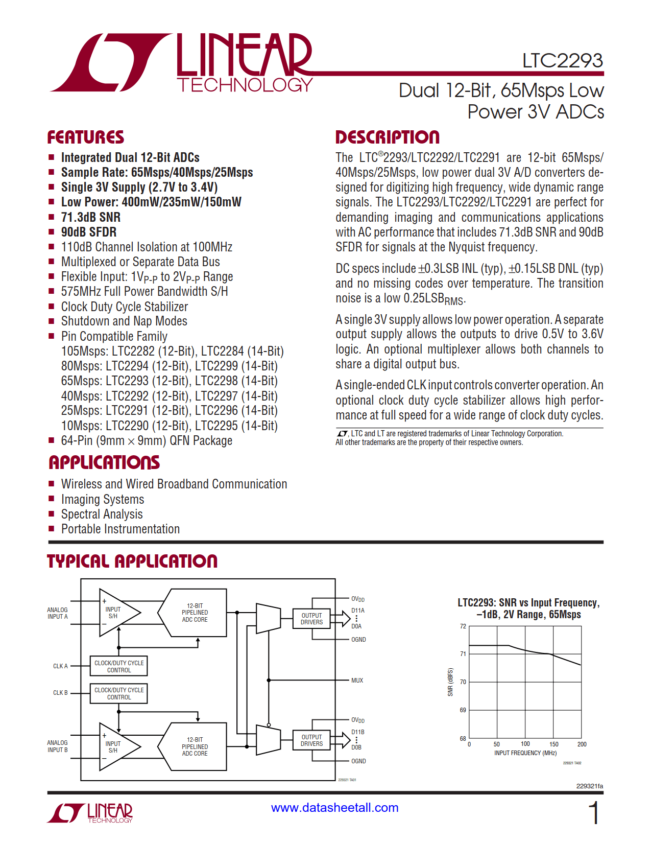
The LTC2293 are 12-bit 65Msps, low power dual 3V A/D converters designed for digitizing high frequency, wide dynamic range signals. The LTC2293 are perfect for demanding imaging and communications applications with AC performance that includes 71.3dB SNR and 90dB SFDR for signals at the Nyquist frequency.
DC specs include ±0.3LSB INL (typ), ±0.15LSB DNL (typ) and no missing codes over temperature. The transition noise is a low 0.25LSBRMS.
A single 3V supply allows low power operation. A separate output supply allows the outputs to drive 0.5V to 3.6V logic. An optional multiplexer allows both channels to share a digital output bus.
A single-ended CLK input controls converter operation. An optional clock duty cycle stabilizer allows high performance at full speed for a wide range of clock duty cycles.
| Part Number | Description |
| LTC1748 | 14-Bit, 80Msps 5V ADC |
| LTC1750 | 14-Bit, 80Msps, 5V Wideband ADC |
| LT1993-2 | High Speed Differential Op Amp |
| LT1994 | Low Noise, Low Distortion Fully Differential Input/Output Amplifier/Driver |
| LTC2202 | 16-Bit, 10Msps, 3.3V ADC, Lowest Noise |
| LTC2208 | 16-Bit, 130Msps, 3.3V ADC, LVDS Outputs |
| LTC2220-1 | 12-Bit, 185Msps, 3.3V ADC, LVDS Outputs |
| LTC2224 | 12-Bit, 135Msps, 3.3V ADC, High IF Sampling |
| LTC2255 | 14-Bit, 125Msps, 3V ADC, Lowest Power |
| LTC2280 | 10-Bit, Dual, 105Msps, 3V ADC, Low Crosstalk |
| LTC2282 | 12-Bit, Dual, 105Msps, 3V ADC, Low Crosstalk |
| LTC2284 | 14-Bit, Dual, 105Msps, 3V ADC, Low Crosstalk |
| LTC2286 | 10-Bit, Dual, 25Msps, 3V ADC, Low Crosstalk |
| LTC2287 | 10-Bit, Dual, 40Msps, 3V ADC, Low Crosstalk |
| LTC2288 | 10-Bit, Dual, 65Msps, 3V ADC, Low Crosstalk |
| LTC2289 | 10-Bit, Dual, 80Msps, 3V ADC, Low Crosstalk |
| LTC2290 | 12-Bit, Dual, 10Msps, 3V ADC, Low Crosstalk |
| LTC2291 | 12-Bit, Dual, 25Msps, 3V ADC, Low Crosstalk |
| LTC2292 | 12-Bit, Dual, 40Msps, 3V ADC, Low Crosstalk |
| LTC2293 | 12-Bit, Dual, 65Msps, 3V ADC, Low Crosstalk |
| LTC2294 | 12-Bit, Dual, 80Msps, 3V ADC, Low Crosstalk |
| LTC2295 | 14-Bit, Dual, 10Msps, 3V ADC, Low Crosstalk |
| LTC2296 | 14-Bit, Dual, 25Msps, 3V ADC, Low Crosstalk |
| LTC2297 | 14-Bit, Dual, 40Msps, 3V ADC, Low Crosstalk |
| LTC2298 | 14-Bit, Dual, 65Msps, 3V ADC, Low Crosstalk |
| LTC2299 | 14-Bit, Dual, 80Msps, 3V ADC, Low Crosstalk |
| LT5512 | DC-3GHz High Signal Level Downconverting Mixer |
| LT5514 | Ultralow Distortion IF Amplifier/ADC Driver with Digitally Controlled Gain |
| LT5515 | 1.5GHz to 2.5GHz Direct Conversion Quadrature Demodulator |
| LT5516 | 800MHz to 1.5GHz Direct Conversion Quadrature Demodulator |
| LT5517 | 40MHz to 900MHz Direct Conversion Quadrature Demodulator |
| LT5522 | 600MHz to 2.7GHz High Linearity Downconverting Mixer |