LTC2233 Datasheet
10-Bit, 80Msps ADCs
10-Bit, 80Msps ADCs
| Part No. | In Stock | Price | Packaging | SPQ | Marking | MSL | Pins | Temp Range | Package Description |
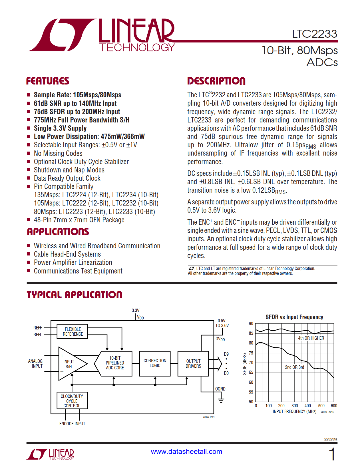
The LTC2233 are 80Msps, sampling 10-bit A/D converters designed for digitizing high frequency, wide dynamic range signals. The LTC2233 are perfect for demanding communications applications with AC performance that includes 61dB SNR and 75dB spurious free dynamic range for signals up to 200MHz. Ultralow jitter of 0.15psRMS allows undersampling of IF frequencies with excellent noise performance.
DC specs include ±0.15LSB INL (typ), ±0.1LSB DNL (typ) and ±0.8LSB INL, ±0.6LSB DNL over temperature. The transition noise is a low 0.12LSBRMS.
A separate output power supply allows the outputs to drive 0.5V to 3.6V logic.
The ENC+ and ENC– inputs may be driven differentially or single ended with a sine wave, PECL, LVDS, TTL, or CMOS inputs. An optional clock duty cycle stabilizer allows high performance at full speed for a wide range of clock duty cycles.