LTC2204 Datasheet
16-Bit, 40Msps ADC
16-Bit, 40Msps ADC
| Part No. | In Stock | Price | Packaging | SPQ | Marking | MSL | Pins | Temp Range | Package Description |
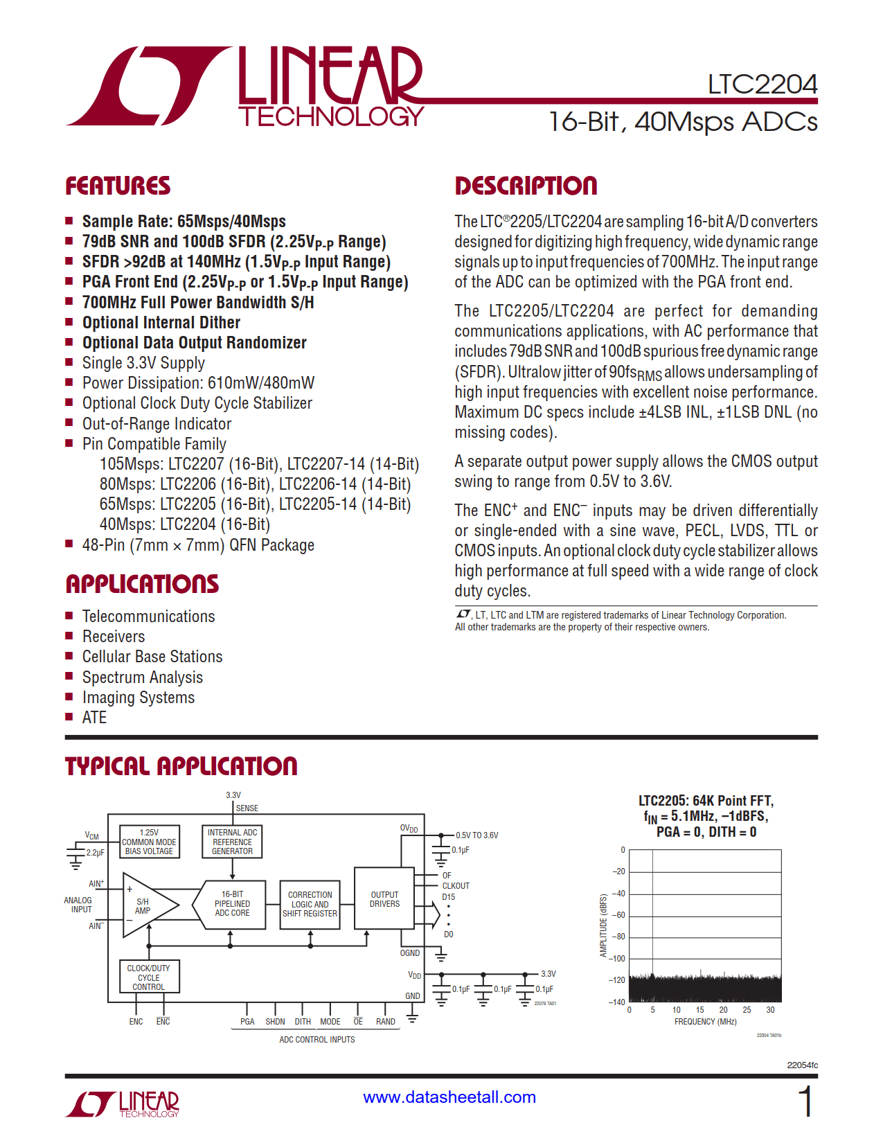
The LTC2204 are sampling 16-bit A/D converters designed for digitizing high frequency, wide dynamic range signals up to input frequencies of 700MHz. The input range of the ADC can be optimized with the PGA front end.
The LTC2204 are perfect for demanding communications applications, with AC performance that includes 79dB SNR and 100dB spurious free dynamic range (SFDR). Ultralow jitter of 90fsRMS allows undersampling of high input frequencies with excellent noise performance. Maximum DC specs include ±4LSB INL, ±1LSB DNL (no missing codes). A separate output power supply allows the CMOS output swing to range from 0.5V to 3.6V.
The ENC+ and ENC– inputs may be driven differentially or single-ended with a sine wave, PECL, LVDS, TTL or CMOS inputs. An optional clock duty cycle stabilizer allows high performance at full speed with a wide range of clock duty cycles.