LTC2185 Datasheet
16-Bit, 125Msps Low Power Dual ADCs
16-Bit, 125Msps Low Power Dual ADCs
| Part No. | In Stock | Price | Packaging | SPQ | Marking | MSL | Pins | Temp Range | Package Description |
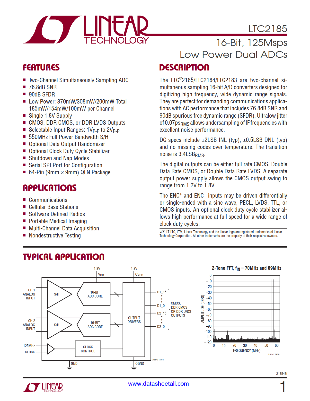
The LTC2185 is two-channel simultaneous sampling 16-bit A/D converters designed for digitizing high frequency, wide dynamic range signals. They are perfect for demanding communications applications with AC performance that includes 76.8dB SNR and 90dB spurious free dynamic range (SFDR). Ultralow jitter of 0.07psRMS allows undersampling of IF frequencies with excellent noise performance.
DC specs include ±2LSB INL (typ), ±0.5LSB DNL (typ) and no missing codes over temperature. The transition noise is 3.4LSBRMS.
The digital outputs can be either full rate CMOS, Double Data Rate CMOS, or Double Data Rate LVDS. A separate output power supply allows the CMOS output swing to range from 1.2V to 1.8V.
The ENC+ and ENC– inputs may be driven differentially or single-ended with a sine wave, PECL, LVDS, TTL, or CMOS inputs. An optional clock duty cycle stabilizer allows high performance at full speed for a wide range of clock duty cycles.