LTC2052 Datasheet
Quad Zero-Drift Operational Amplifiers
Quad Zero-Drift Operational Amplifiers
| Part No. | In Stock | Price | Packaging | SPQ | Marking | MSL | Pins | Temp Range | Package Description |
The LTC2052 are quad zero-drift operational amplifiers available in the MS8 and SO-8/GN16 and S14 packages. It operate from a single 2.7V supply and support ±5V applications. The current consumption is 750µA per op amp.
The LTC2052, despite their miniature size, feature uncompromising DC performance. The typical input offset voltage and offset drift are 0.5µV and 10nV/°C. The almost zero DC offset and drift are supported with a power supply rejection ratio (PSRR) and common mode rejection ratio (CMRR) of more than 130dB.
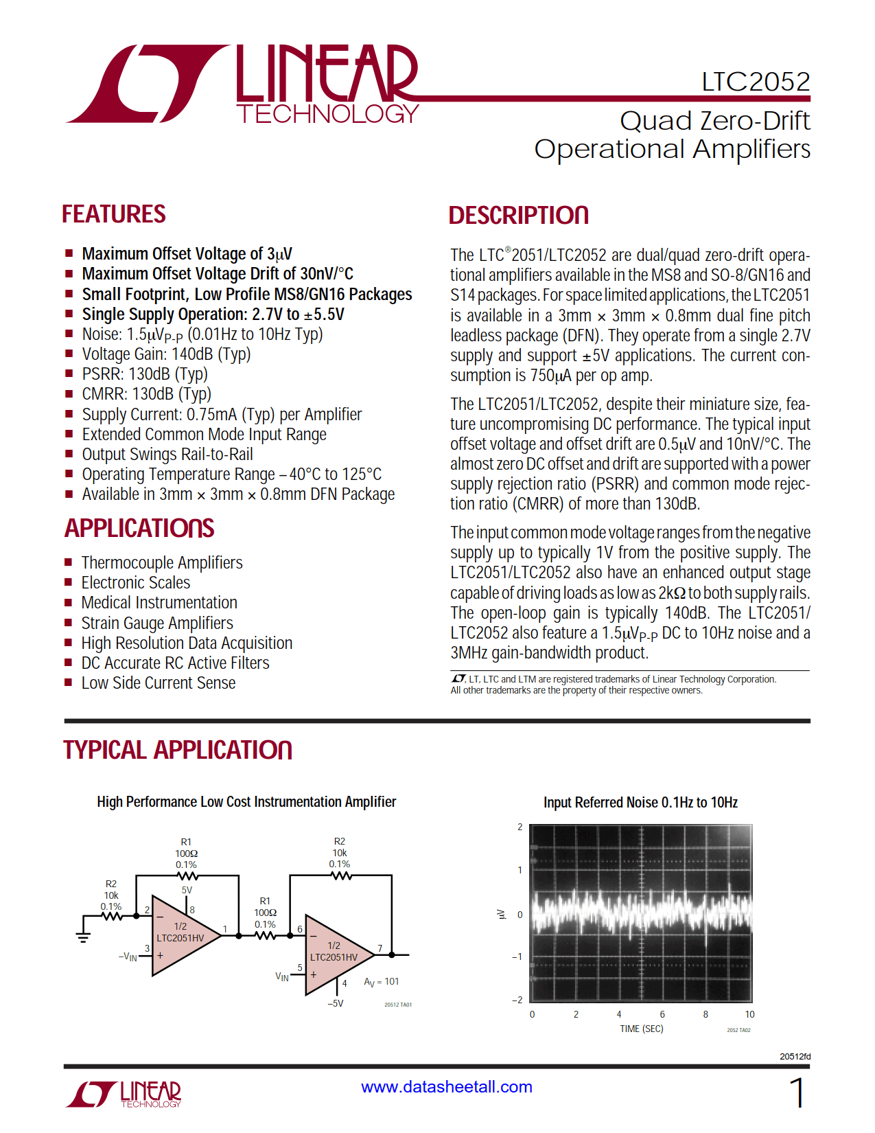
The input common mode voltage ranges from the negative supply up to typically 1V from the positive supply. The LTC2052 also have an enhanced output stage capable of driving loads as low as 2kΩ to both supply rails. The open-loop gain is typically 140dB. The LTC2052 also feature a 1.5µVP-P DC to 10Hz noise and a 3MHz gain-bandwidth product.