ADV7125 Datasheet

330MHz Triple 8-Bit High Speed Video DAC

Part No.:
ADV7125
Manufacturer:
Analog Devices, Inc.
Page:
17 Pages
Size:
372 KB
Views:
1
Update Time:
2025-01-09 17:37:23

ADV7125 DataSheet Applicable Part

Part No. In Stock Price Packaging SPQ Marking MSL Pins Temp Range Package Description
SPQ:Standard Pack Quantity;MSL:Moisture Sensitivity Level

ADV7125 DataSheet PDF

ADV7125 Features

  • 330 MSPS throughput rate
  • Triple 8-bit DACs
  • RS-343A-/RS-170-compatible output
  • Complementary outputs
  • DAC output current range: 2.0 mA to 26.5 mA
  • TTL-compatible inputs
  • Internal reference (1.235 V)
  • Single-supply +5 V/+3.3 V operation
  • 48-lead LQFP and LFCSP
  • Low power dissipation (30 mW minimum at 3 V)
  • Low power standby mode (6 mW typical at 3 V)
  • Industrial temperature range (−40°C to +85°C)
  • RoHS compliant packages
  • Qualified for automotive applications

ADV7125 Applications

  • Digital video systems
  • High resolution color graphics
  • Digital radio modulation
  • Image processing
  • Instrumentation
  • Video signal reconstruction
  • Automotive infotainment units

ADV7125 Description

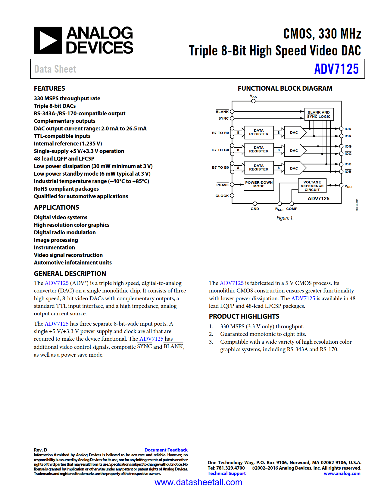
The ADV7125 (ADV®) is a triple high speed, digital-to-analog converter (DAC) on a single monolithic chip. It consists of three high speed, 8-bit video DACs with complementary outputs, a standard TTL input interface, and a high impedance, analog output current source.

The ADV7125 has three separate 8-bit-wide input ports. A single +5 V/+3.3 V power supply and clock are all that are required to make the device functional. The ADV7125 has additional video control signals, composite SYNC and BLANK as well as a power save mode.

The ADV7125 is fabricated in a 5 V CMOS process. Its monolithic CMOS construction ensures greater functionality with lower power dissipation. The ADV7125 is available in 48- lead LQFP and 48-lead LFCSP packages.

ADV7125 Datasheet FAQs