ADUC836 Datasheet
MicroConverter® , Dual 16-Bit Sigma-Delta ADCs with Embedded 62 kB Flash MCU
MicroConverter® , Dual 16-Bit Sigma-Delta ADCs with Embedded 62 kB Flash MCU
| Part No. | In Stock | Price | Packaging | SPQ | Marking | MSL | Pins | Temp Range | Package Description |
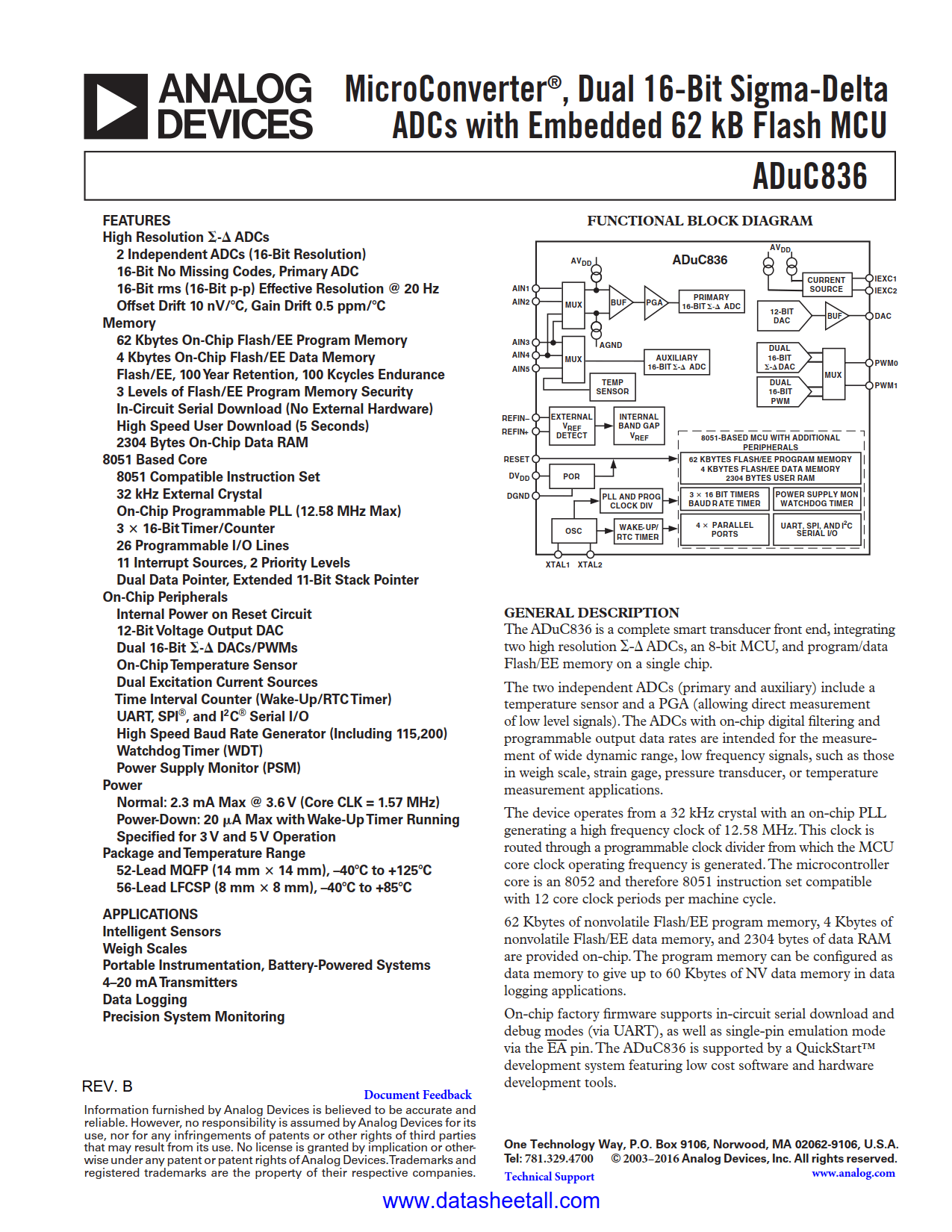
The ADuC836 is a complete smart transducer front end, integrating two high resolution Σ-Δ ADCs, an 8-bit MCU, and program/data Flash/EE memory on a single chip.
The two independent ADCs (primary and auxiliary) include a temperature sensor and a PGA (allowing direct measurement of low level signals). The ADCs with on-chip digital filtering and programmable output data rates are intended for the measurement of wide dynamic range, low frequency signals, such as those in weigh scale, strain gage, pressure transducer, or temperature measurement applications.
The device operates from a 32 kHz crystal with an on-chip PLL generating a high frequency clock of 12.58 MHz. This clock is routed through a programmable clock divider from which the MCU core clock operating frequency is generated. The microcontroller core is an 8052 and therefore 8051 instruction set compatible with 12 core clock periods per machine cycle.
62 Kbytes of nonvolatile Flash/EE program memory, 4 Kbytes of nonvolatile Flash/EE data memory, and 2304 bytes of data RAM are provided on-chip. The program memory can be configured as data memory to give up to 60 Kbytes of NV data memory in data logging applications.
On-chip factory firmware supports in-circuit serial download and debug modes (via UART), as well as single-pin emulation mode via the EA pin. The ADuC836 is supported by a QuickStart™ development system featuring low cost software and hardware development tools.