ADP5053 Datasheet
Integrated Power Solution with Quad Buck Regulators and Supervisory Circuits
Integrated Power Solution with Quad Buck Regulators and Supervisory Circuits
| Part No. | In Stock | Price | Packaging | SPQ | Marking | MSL | Pins | Temp Range | Package Description |
| ADP5053ACPZ-R7 | 1500pcs | $5.769 | Reel | 750 | ADP5053ACPZ | 3 | 48 | -40°C ~ 125°C | 48-Lead LFCSP |
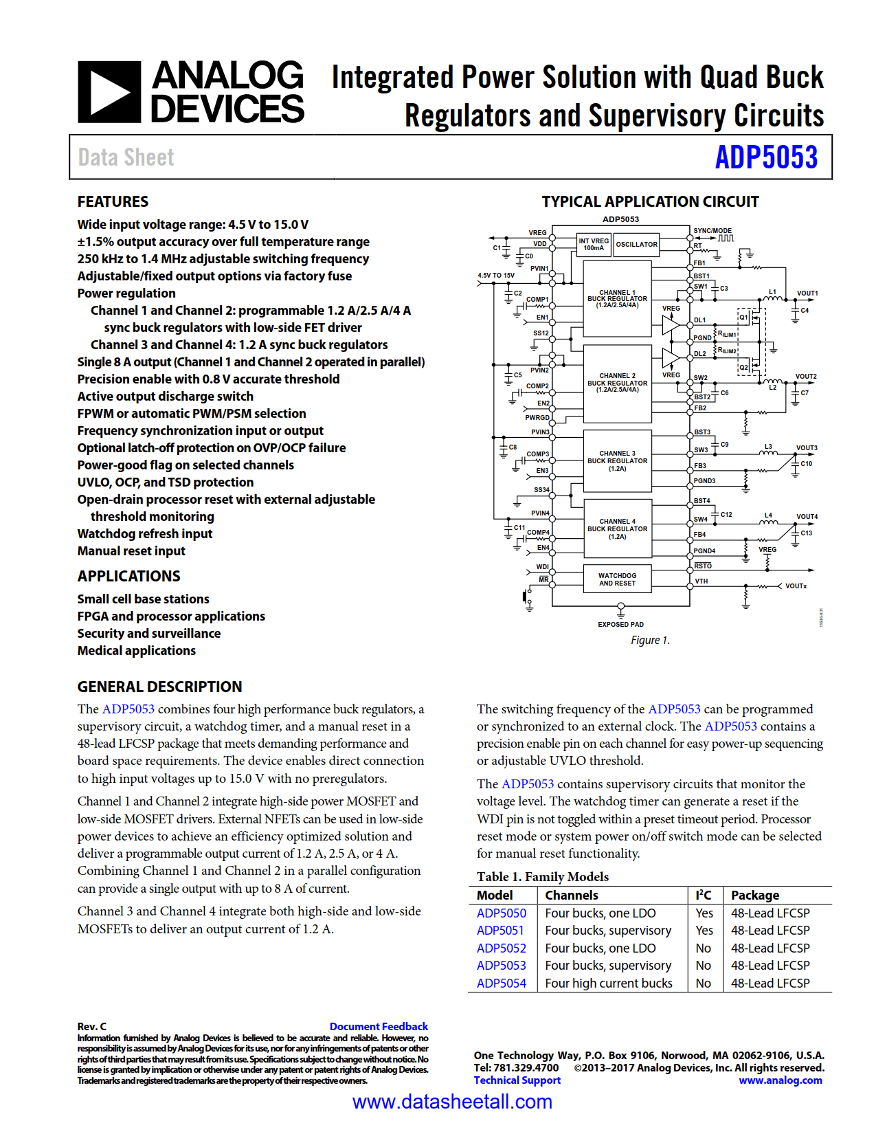
The ADP5053 combines four high performance buck regulators, a supervisory circuit, a watchdog timer, and a manual reset in a 48-lead LFCSP package that meets demanding performance and board space requirements. The device enables direct connection to high input voltages up to 15.0 V with no preregulators.
Channel 1 and Channel 2 integrate high-side power MOSFET and low-side MOSFET drivers. External NFETs can be used in low-side power devices to achieve an efficiency optimized solution and deliver a programmable output current of 1.2 A, 2.5 A, or 4 A. Combining Channel 1 and Channel 2 in a parallel configuration can provide a single output with up to 8 A of current.
Channel 3 and Channel 4 integrate both high-side and low-side MOSFETs to deliver an output current of 1.2 A.
The switching frequency of the ADP5053 can be programmed or synchronized to an external clock. The ADP5053 contains a precision enable pin on each channel for easy power-up sequencing or adjustable UVLO threshold.
The ADP5053 contains supervisory circuits that monitor the voltage level. The watchdog timer can generate a reset if the WDI pin is not toggled within a preset timeout period. Processor reset mode or system power on/off switch mode can be selected for manual reset functionality.