ADP5050 Datasheet
5-Channel Integrated Power Solution with Quad Buck Regulators, 200 mA LDO Regulator and I2C interface
5-Channel Integrated Power Solution with Quad Buck Regulators, 200 mA LDO Regulator and I2C interface
| Part No. | In Stock | Price | Packaging | SPQ | Marking | MSL | Pins | Temp Range | Package Description |
| ADP5050ACPZ-R7 | 1440pcs | $6.687 | Reel | 750 | ADP5050ACPZ | 3 | 48 | -40°C ~ 125°C | 48-Lead LFCSP |
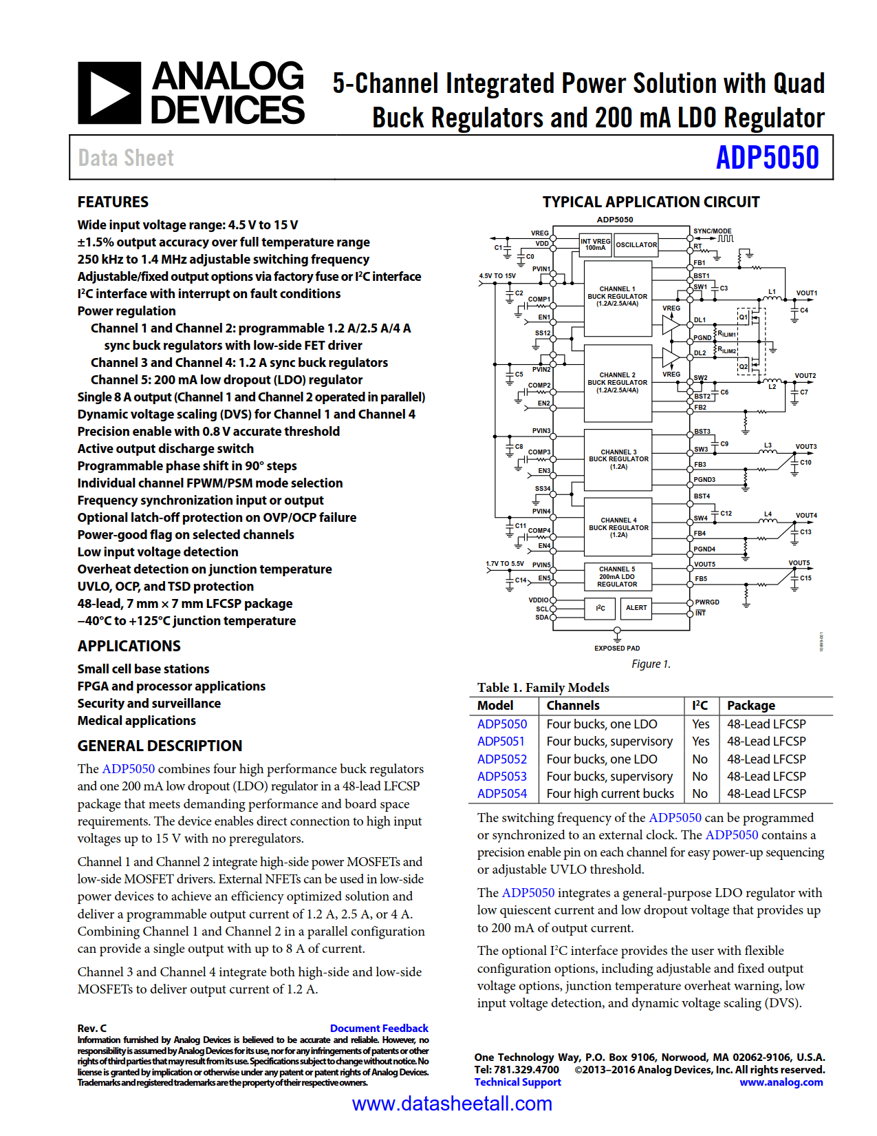
The ADP5050 combines four high performance buck regulators and one 200 mA low dropout (LDO) regulator in a 48-lead LFCSP package that meets demanding performance and board space requirements. The device enables direct connection to high input voltages up to 15 V with no preregulators.
Channel 1 and Channel 2 integrate high-side power MOSFETs and low-side MOSFET drivers. External NFETs can be used in low-side power devices to achieve an efficiency optimized solution and deliver a programmable output current of 1.2 A, 2.5 A, or 4 A. Combining Channel 1 and Channel 2 in a parallel configuration can provide a single output with up to 8 A of current.
Channel 3 and Channel 4 integrate both high-side and low-side MOSFETs to deliver output current of 1.2 A.
The switching frequency of the ADP5050 can be programmed or synchronized to an external clock. The ADP5050 contains a precision enable pin on each channel for easy power-up sequencing or adjustable UVLO threshold.
The ADP5050 integrates a general-purpose LDO regulator with low quiescent current and low dropout voltage that provides up to 200 mA of output current.
The optional I2C interface provides the user with flexible configuration options, including adjustable and fixed output voltage options, junction temperature overheat warning, low input voltage detection, and dynamic voltage scaling (DVS).