ADP198 Datasheet
Logic-Controlled, 1 A, High-Side Load Switch with Reverse Current Blocking
Logic-Controlled, 1 A, High-Side Load Switch with Reverse Current Blocking
| Part No. | In Stock | Price | Packaging | SPQ | Marking | MSL | Pins | Temp Range | Package Description |
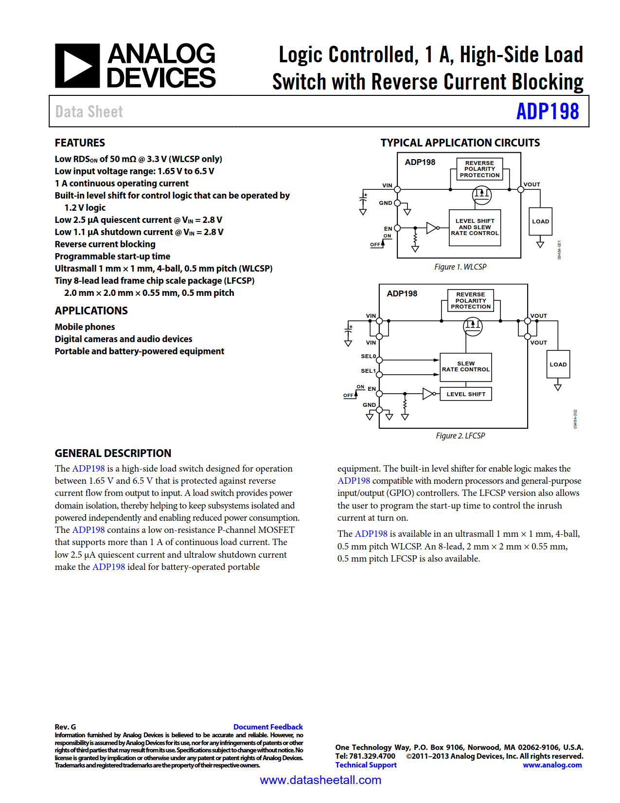
The ADP198 is a high-side load switch designed for operation between 1.65 V to 6.5 V that is protected against reverse current flow from output to input. A load switch provides power domain isolation thereby helping to keep subsystems isolated and powered independently, and enabling reduced power consumption. The ADP198 contains a low on-resistance Pchannel MOSFET that supports over 1 Amp of continuous load current. The low 2.5μA quiescent current and ultra-low shutdown current make the ADP198 ideal for battery-operated portable equipment. The built-in level shifter for enable logic makes the ADP198 compatible with modern processors and GPIO controllers. The LFCSP version also allows the user to program the start up time which control the inrush current at turn on.
The ADP198 is available in an ultrasmall 1 mm × 1 mm, 4-ball, 0.5 mm pitch WLCSP. An 8-Lead 2 mm x 2 mm x 0.55 mm, 0.5 mm pitch LFCSP is also available.