ADG612 Datasheet

1 pC Charge Injection, 100 pA Leakage, CMOS, ±5 V/+5 V/+3 V, Quad SPST Switches

Part No.:
ADG612
Manufacturer:
Analog Devices, Inc.
Page:
16 Pages
Size:
262 KB
Views:
0
Update Time:
2026-02-11 14:13:00

ADG612 DataSheet Applicable Part

Part No. In Stock Price Packaging SPQ Marking MSL Pins Temp Range Package Description
SPQ:Standard Pack Quantity;MSL:Moisture Sensitivity Level

ADG612 DataSheet PDF

ADG612 Features

  • 1 pC Charge Injection
  • ±2.7 V to ±5.5 V dual-supply operation
  • +2.7 V to +5.5 V single-supply operation
  • Automotive temperature range: −40°C to +125°C
  • 100 pA maximum at 25°C leakage currents
  • 85 Ω on resistance
  • Rail-to-rail switching operation
  • Fast switching times
  • 16-lead TSSOP and SOIC packages
  • Typical power consumption: <0.1 μW
  • TTL-/CMOS-compatible inputs

ADG612 Applications

  • Automatic test equipment
  • Data acquisition systems
  • Battery-powered systems
  • Communications systems
  • Sample-and-hold systems
  • Audio signal routing
  • Relay replacement
  • Avionics

ADG612 Description

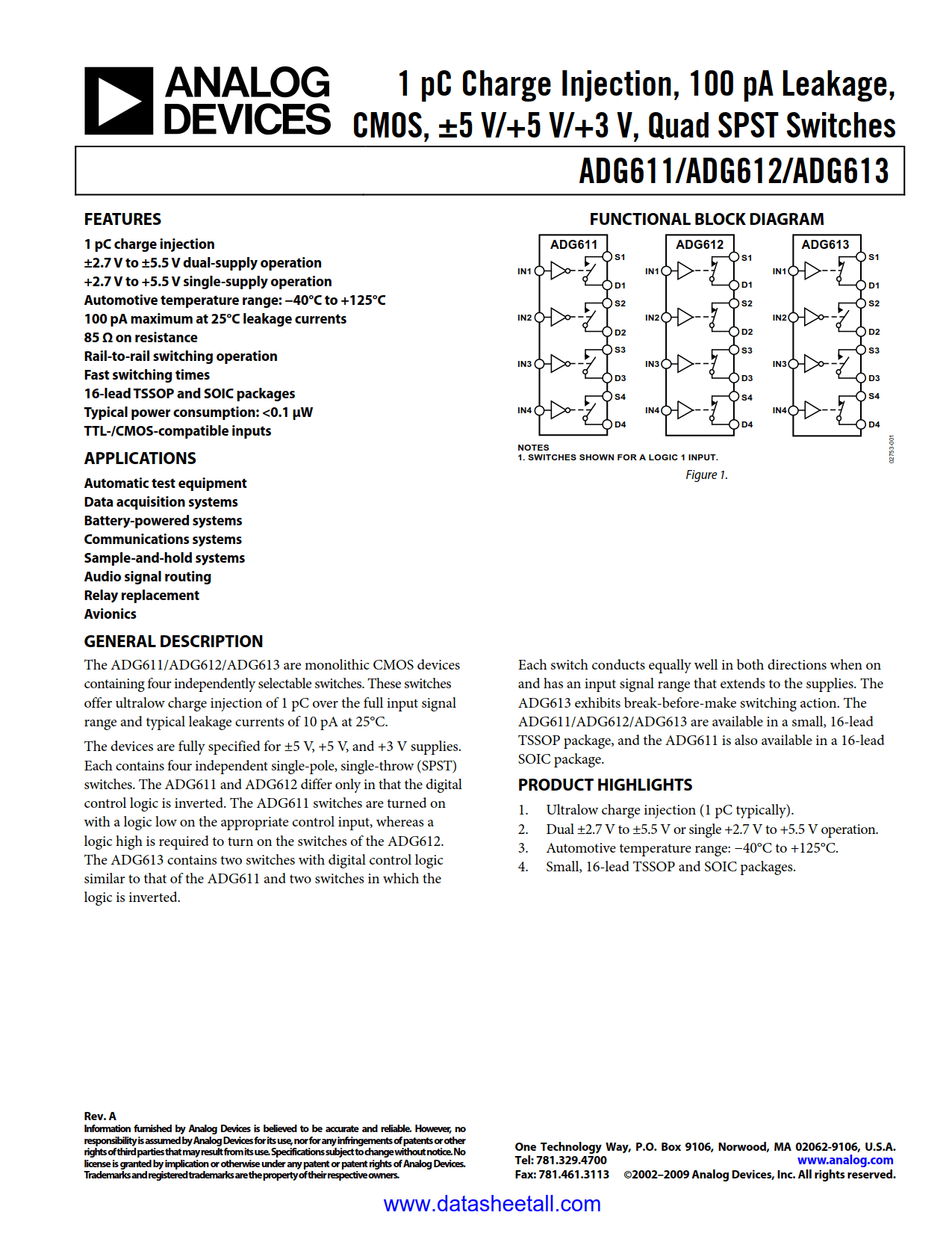
The ADG612 are monolithic CMOS devices containing four independently selectable switches. These switches offer ultralow charge injection of 1 pC over the full input signal range and typical leakage currents of 10 pA at 25°C.

The devices are fully specified for ±5 V, +5 V, and +3 V supplies. Each contains four independent single-pole, single-throw (SPST) switches. The ADG612 differ only in that the digital control logic is inverted. A logic high is required to turn on the switches of the ADG612.

Each switch conducts equally well in both directions when on and has an input signal range that extends to the supplies. The ADG612 are available in a small, 16-lead TSSOP package.

PRODUCT HIGHLIGHTS

  1. Ultralow charge injection (1 pC typically).
  2. Dual ±2.7 V to ±5.5 V or single +2.7 V to +5.5 V operation.
  3. Automotive temperature range: −40°C to +125°C.
  4. Small, 16-lead TSSOP and SOIC packages.

ADG612 Datasheet FAQs