ADG406 Datasheet
LC2MOS ± 15V 16 Channel High Performance Analog Multiplexer

LC2MOS ± 15V 16 Channel High Performance Analog Multiplexer
| Part No. | In Stock | Price | Packaging | SPQ | Marking | MSL | Pins | Temp Range | Package Description |
| ADG406BNZ | 0 | $11.799 | Tube | 13 | ADG406BNZ | 1 | 28 | -40°C ~ 85°C | 28-Lead PDIP |
| ADG406BPZ | 156pcs | $10.611 | Tube | 39 | ADG406BPZ | 3 | 28 | -40°C ~ 85°C | 28-Lead PLCC |
| ADG406BPZ-REEL | 750pcs | $10.611 | Reel | 750 | ADG406BPZ | 3 | 28 | -40°C ~ 85°C | 28-Lead PLCC |
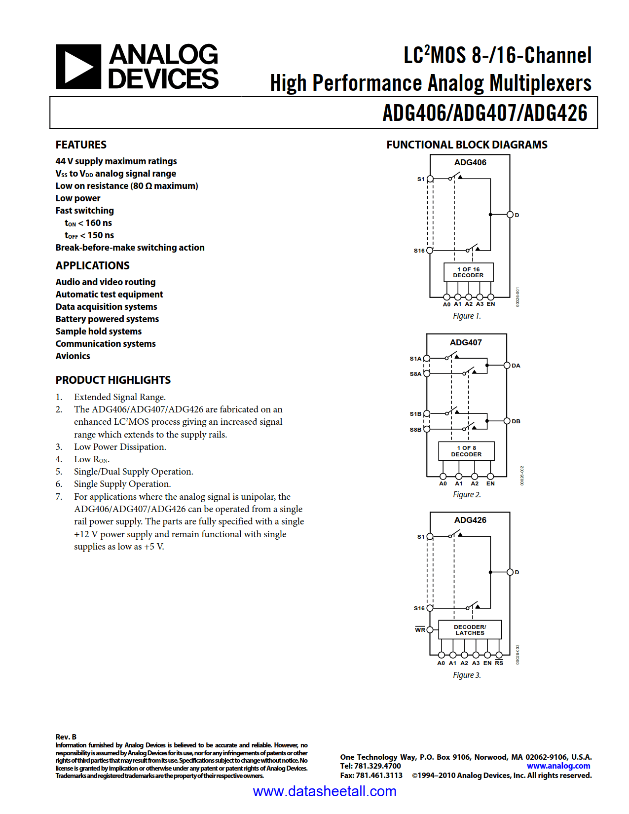
The ADG406 are monolithic CMOS analog multiplexers. The ADG406 switch one of sixteen inputs to a common output as determined by the 4-bit binary address lines: A0, A1, A2, and A3. An EN input on all devices is used to enable or disable the device. When disabled, all channels are switched off.
The ADG406 are designed on an enhanced LC2MOS process that provides low power dissipation yet gives high switching speed and low on resistance. These features make the parts suitable for high speed data acquisition systems and audio signal switching. Low power dissipation makes the parts suitable for battery powered systems. Each channel conducts equally well in both directions when on and has an input signal range which extends to the supplies. In the off condition, signal levels up to the supplies are blocked. All channels exhibit break-before-make switching action preventing momentary shorting when switching channels. Inherent in the design is low charge injection for minimum transients when switching the digital inputs.