ADF4377 Datasheet
Microwave Wideband Synthesizer with Integrated VCO
Microwave Wideband Synthesizer with Integrated VCO
| Part No. | In Stock | Price | Packaging | SPQ | Marking | MSL | Pins | Temp Range | Package Description |
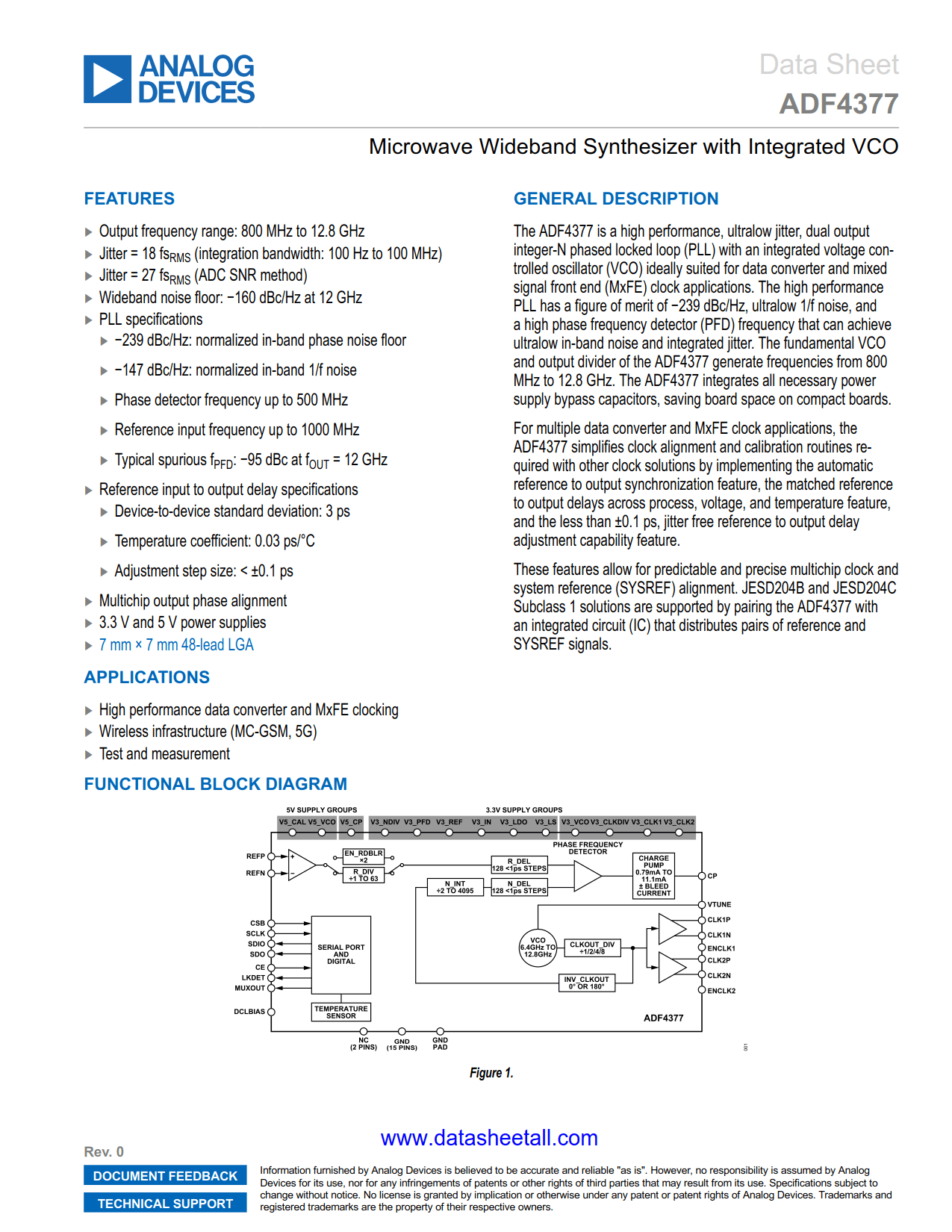
The ADF4377 is a high performance, ultralow jitter, dual output integer-N phased locked loop (PLL) with an integrated voltage controlled oscillator (VCO) ideally suited for data converter and mixed signal front end (MxFE) clock applications. The high performance PLL has a figure of merit of −239 dBc/Hz, ultralow 1/f noise, and a high phase frequency detector (PFD) frequency that can achieve ultralow in-band noise and integrated jitter. The fundamental VCO and output divider of the ADF4377 generate frequencies from 800 MHz to 12.8 GHz. The ADF4377 integrates all necessary power supply bypass capacitors, saving board space on compact boards.
For multiple data converter and MxFE clock applications, the ADF4377 simplifies clock alignment and calibration routines required with other clock solutions by implementing the automatic reference to output synchronization feature, the matched reference to output delays across process, voltage, and temperature feature, and the less than ±0.1 ps, jitter free reference to output delay adjustment capability feature.
These features allow for predictable and precise multichip clock and system reference (SYSREF) alignment. JESD204B and JESD204C Subclass 1 solutions are supported by pairing the ADF4377 with an integrated circuit (IC) that distributes pairs of reference and SYSREF signals.