ADF4111 Datasheet
Single, Integer-N, 1.2 GHz PLL With Programmable Prescaler And Charge Pump
Single, Integer-N, 1.2 GHz PLL With Programmable Prescaler And Charge Pump
| Part No. | In Stock | Price | Packaging | SPQ | Marking | MSL | Pins | Temp Range | Package Description |
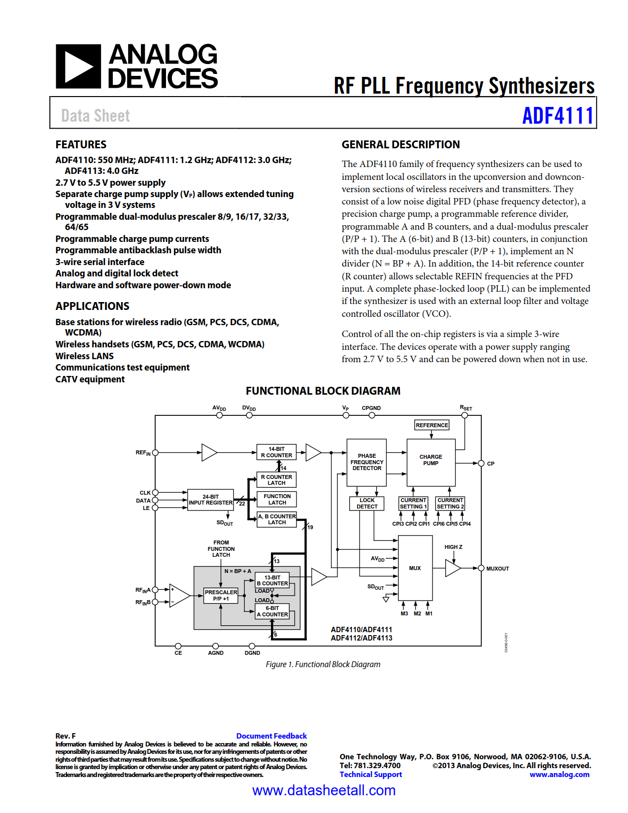
The ADF4111 family of frequency synthesizers can be used to implement local oscillators in the up-conversion and down-conversion sections of wireless receivers and transmitters. They consist of low-noise digital PFD (Phase Frequency Detector), a precision charge pump, a programmable reference divider, programmable A and B counters and a dual modulus prescaler (P/P+1). The A (6-bit) and B (13-bit) counters, in conjunction with the dual modulus prescaler (P/P+1), implement an N divider (N = BP+A). In addition, the 14-bit reference counter (R Counter), allows selectable REFIN frequencies at the PFD input. A complete PLL (Phase-Locked Loop) can be implemented if the synthesizer is used with an external loop filter and VCO (Voltage Controlled Oscillator).
Control of all the on-chip registers is via a simple 3-wire interface. The devices operate with a power supply ranging from 2.7 V to 5.5 V and can be powered down when not in use.