ADCLK954 Datasheet
Two Selectable Inputs, 12 LVPECL Outputs, SiGe Clock Fanout Buffer
Two Selectable Inputs, 12 LVPECL Outputs, SiGe Clock Fanout Buffer
| Part No. | In Stock | Price | Packaging | SPQ | Marking | MSL | Pins | Temp Range | Package Description |
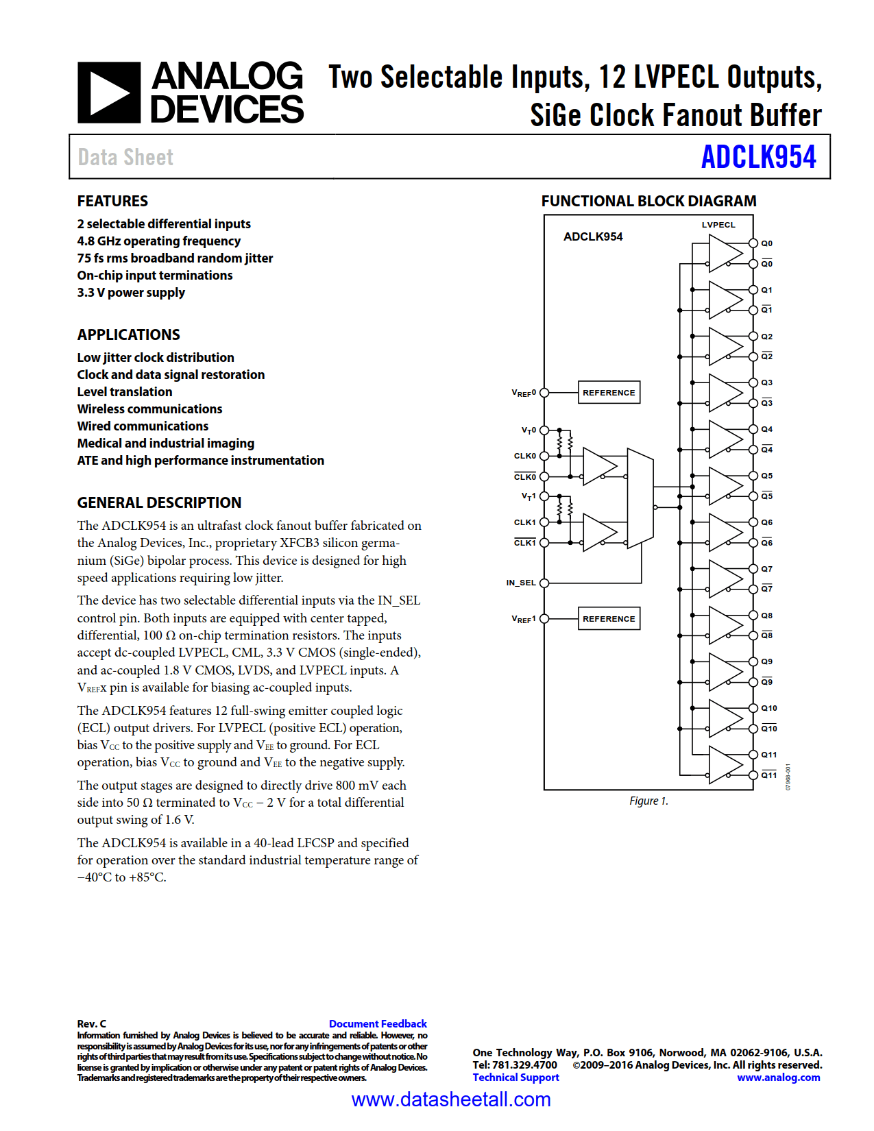
The ADCLK954 is an ultrafast clock fanout buffer fabricated on the Analog Devices, Inc., proprietary XFCB3 silicon germanium (SiGe) bipolar process. This device is designed for high speed applications requiring low jitter.
The device has two selectable differential inputs via the IN_SEL control pin. Both inputs are equipped with center tapped, differential, 100 Ω on-chip termination resistors. The inputs accept dc-coupled LVPECL, CML, 3.3 V CMOS (single-ended), and ac-coupled 1.8 V CMOS, LVDS, and LVPECL inputs. A VREFx pin is available for biasing ac-coupled inputs.
The ADCLK954 features 12 full-swing emitter coupled logic (ECL) output drivers. For LVPECL (positive ECL) operation, bias Vcc to the positive supply and VEE to ground. For ECL operation, bias VCC to ground and VEE to the negative supply.
The output stages are designed to directly drive 800 mV each side into 50 Ω terminated to VCC − 2 V for a total differential output swing of 1.6 V.
The ADCLK954 is available in a 40-lead LFCSP and specified for operation over the standard industrial temperature range of −40°C to +85°C.