AD9776 Datasheet

Dual 12-Bit, 1 GSPS, Digital-to-Analog Converter

Part No.:
AD9776
Manufacturer:
Analog Devices, Inc.
Page:
56 Pages
Size:
1207 KB
Views:
1
Update Time:
2025-01-06 15:10:46

AD9776 DataSheet Applicable Part

Part No. In Stock Price Packaging SPQ Marking MSL Pins Temp Range Package Description
SPQ:Standard Pack Quantity;MSL:Moisture Sensitivity Level

AD9776 DataSheet PDF

AD9776 Features

  • Low power: 1.0 W @ 1 GSPS, 600 mW @ 500 MSPS, full operating conditions
  • SFDR = 78 dBc to fOUT = 100 MHz
  • Single carrier WCDMA ACLR = 79 dBc @ 80 MHz IF
  • Analog output: adjustable 8.7 mA to 31.7 mA, RL = 25 Ω to 50 Ω
  • Auxiliary DACs allow control of external VGA and offset control
  • Multiple chip synchronization interface
  • High performance, low noise PLL clock multiplier
  • Digital inverse sinc filter
  • 100-lead, exposed paddle TQFP package
  • See datasheet for additional features

AD9776 Applications

  • Wireless infrastructure
    WCDMA, CDMA2000, TD-SCDMA, WiMax, GSM
  • Digital high or low IF synthesis
  • Internal digital upconversion capability
  • Transmit diversity
  • Wideband communications: LMDS/MMDS, point-to-point

AD9776 Description

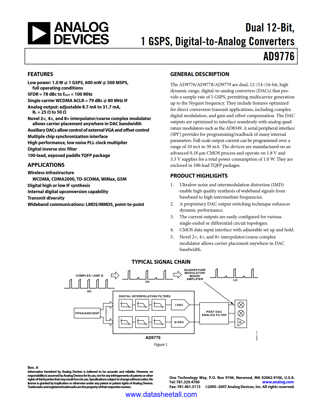
The AD9776 are dual, 12-bit, high dynamic range, digital-to-analog converters (DACs) that provide a sample rate of 1 GSPS, permitting multicarrier generation up to the Nyquist frequency. They include features optimized for direct conversion transmit applications, including complex digital modulation, and gain and offset compensation. The DAC outputs are optimized to interface seamlessly with analog quadrature modulators such as the AD8349. A serial peripheral interface (SPI®) provides for programming/readback of many internal parameters. Full-scale output current can be programmed over a range of 10 mA to 30 mA. The devices are manufactured on an advanced 0.18 μm CMOS process and operate on 1.8 V and 3.3 V supplies for a total power consumption of 1.0 W. They are enclosed in 100-lead TQFP packages.

AD9776 Datasheet FAQs