AD9516-1 Datasheet
14-Output Clock Generator with Integrated 2.5 GHz VCO
14-Output Clock Generator with Integrated 2.5 GHz VCO
| Part No. | In Stock | Price | Packaging | SPQ | Marking | MSL | Pins | Temp Range | Package Description |
| AD9516-1BCPZ | 0 | $11.376 | Tray | 260 | AD9516-1BCPZ | 3 | 64 | -40°C ~ 85°C | 64-Lead LFCSP-VQ |
| AD9516-1BCPZ-REEL7 | 750pcs | $11.376 | Reel | 750 | AD9516-1BCPZ | 3 | 64 | -40°C ~ 85°C | 64-Lead LFCSP-VQ |
The AD9516-1 provides a multi-output clock distribution function with subpicosecond jitter performance, along with an on-chip PLL and VCO. The on-chip VCO tunes from 2.30 GHz to 2.65 GHz. Optionally, an external VCO/VCXO of up to 2.4 GHz can be used.
The AD9516-1 emphasizes low jitter and phase noise to maximize data converter performance, and it can benefit other applications with demanding phase noise and jitter requirements.
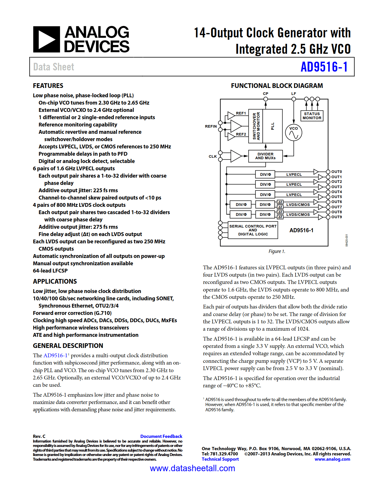
The AD9516-1 features six LVPECL outputs (in three pairs) and four LVDS outputs (in two pairs). Each LVDS output can be reconfigured as two CMOS outputs. The LVPECL outputs operate to 1.6 GHz, the LVDS outputs operate to 800 MHz, and the CMOS outputs operate to 250 MHz.
Each pair of outputs has dividers that allow both the divide ratio and coarse delay (or phase) to be set. The range of division for the LVPECL outputs is 1 to 32. The LVDS/CMOS outputs allow a range of divisions up to a maximum of 1024.
The AD9516-1 is available in a 64-lead LFCSP and can be operated from a single 3.3 V supply. An external VCO, which requires an extended voltage range, can be accommodated by connecting the charge pump supply (VCP) to 5 V. A separate LVPECL power supply can be from 2.5 V to 3.3 V (nominal).
The AD9516-1 is specified for operation over the industrial range of −40°C to +85°C.