AD9266-EP Datasheet
16-Bit, 65 MSPS, 1.8 V Analog-to-Digital Converter
16-Bit, 65 MSPS, 1.8 V Analog-to-Digital Converter
| Part No. | In Stock | Price | Packaging | SPQ | Marking | MSL | Pins | Temp Range | Package Description |
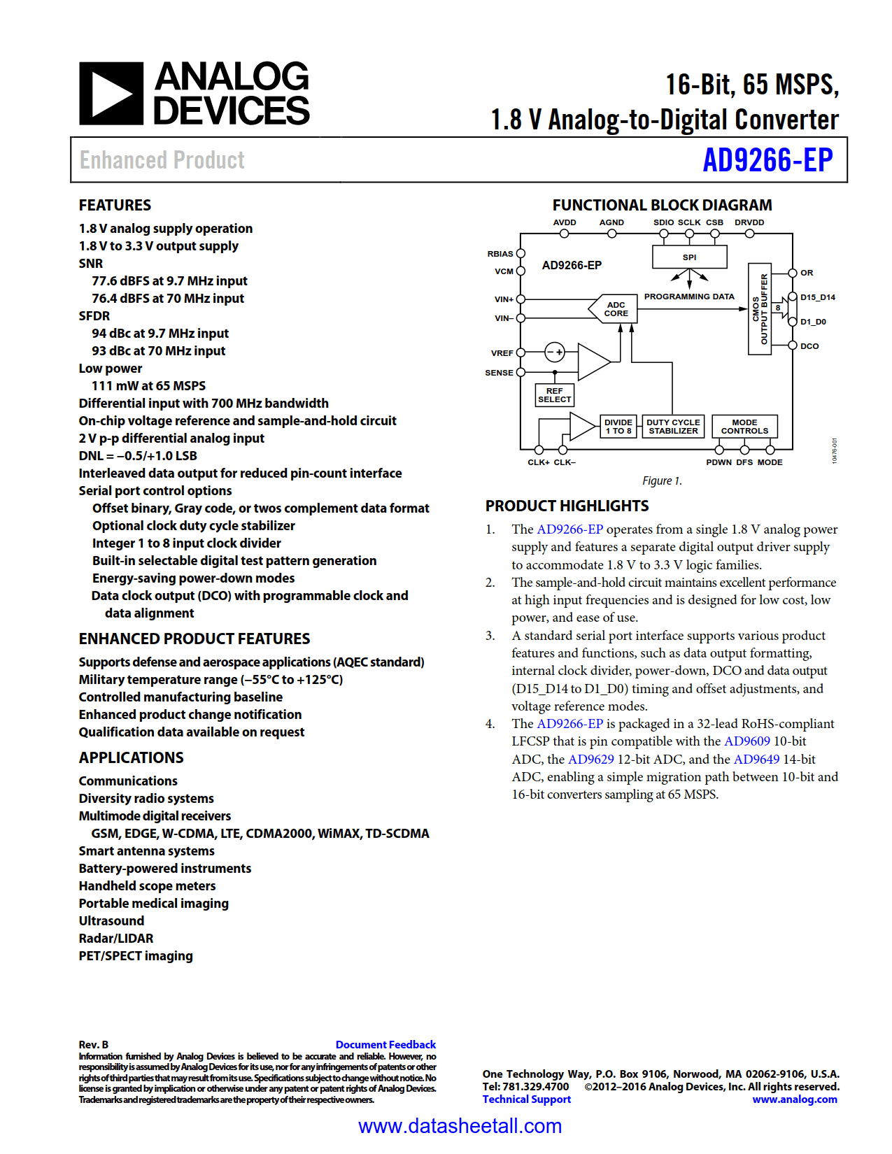
The AD9266-EP is a monolithic, single-channel 1.8 V supply, 16-bit, 65 MSPS analog-to-digital converter (ADC). It features a high performance sample-and-hold circuit and on-chip voltage reference.
The product uses multistage differential pipeline architecture with output error correction logic to provide 16-bit accuracy at 65 MSPS data rates and to guarantee no missing codes over the full operating temperature range.
The ADC contains several features designed to maximize flexibility and minimize system cost, such as programmable clock and data alignment and programmable digital test pattern generation. The available digital test patterns include built-in deterministic and pseudorandom patterns, along with custom user-defined test patterns entered via the serial port interface (SPI).
A differential clock input with a selectable internal 1-to-8 divide ratio controls all internal conversion cycles. An optional duty cycle stabilizer (DCS) compensates for wide variations in the clock duty cycle while maintaining excellent overall ADC performance.
The interleaved digital output data is presented in offset binary, gray code, or twos complement format. A data clock output (DCO) is provided to ensure proper latch timing with receiving logic. CMOS levels from 1.8 V through 3.3 V are supported.
The AD9266-EP is available in a 32-lead RoHS compliant LFCSP and is specified over the −55°C to +125°C temperature range.
Additional application and technical information can be found in the AD9266 data sheet.