AD9218-EP Datasheet
10-Bit, 105 MSPS 3 V Dual Analog-to-Digital Converter
10-Bit, 105 MSPS 3 V Dual Analog-to-Digital Converter
| Part No. | In Stock | Price | Packaging | SPQ | Marking | MSL | Pins | Temp Range | Package Description |
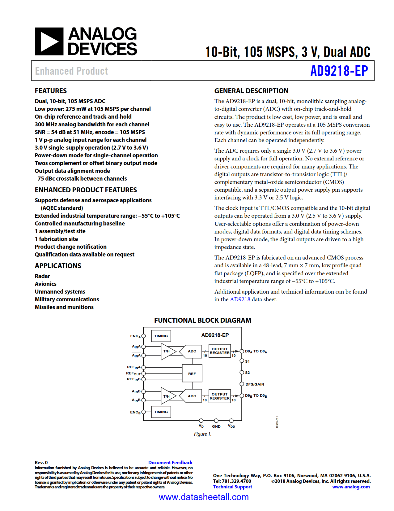
The AD9218-EP is a dual, 10-bit, monolithic sampling analogto-digital converter (ADC) with on-chip track-and-hold circuits. The product is low cost, low power, and is small and easy to use. The AD9218-EP operates at a 105 MSPS conversion rate with dynamic performance over its full operating range. Each channel can be operated independently.
The ADC requires only a single 3.0 V (2.7 V to 3.6 V) power supply and a clock for full operation. No external reference or driver components are required for many applications. The digital outputs are transistor-to-transistor logic (TTL)/complementary metal-oxide semiconductor (CMOS) compatible, and a separate output power supply pin supports interfacing with 3.3 V or 2.5 V logic.
The clock input is TTL/CMOS compatible and the 10-bit digital outputs can be operated from a 3.0 V (2.5 V to 3.6 V) supply. User-selectable options offer a combination of power-down modes, digital data formats, and digital data timing schemes. In power-down mode, the digital outputs are driven to a high impedance state.
The AD9218-EP is fabricated on an advanced CMOS process and is available in a 48-lead, 7 mm × 7 mm, low profile quad flat package (LQFP), and is specified over the extended industrial temperature range of −55°C to +105°C.
Additional application and technical information can be found in the AD9218 data sheet.