AD9215 Datasheet
10-Bit, 65/80/105 MSPS 3 V A/D Converter
10-Bit, 65/80/105 MSPS 3 V A/D Converter
| Part No. | In Stock | Price | Packaging | SPQ | Marking | MSL | Pins | Temp Range | Package Description |
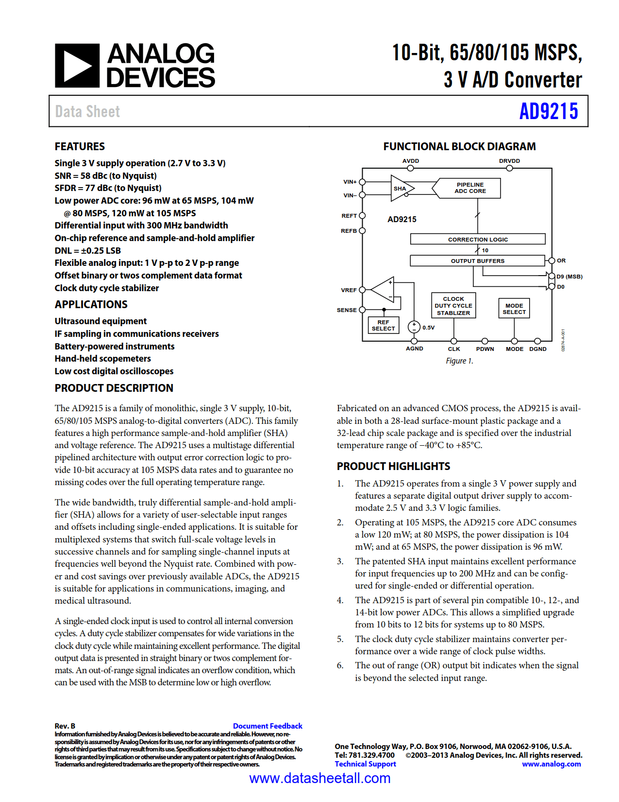
The AD9215 is a family of monolithic, single 3 V supply, 10-bit, 65/80/105 MSPS analog-to-digital converters (ADC). This family features a high performance sample-and-hold amplifier (SHA) and voltage reference. The AD9215 uses a multistage differential pipelined architecture with output error correction logic to provide 10-bit accuracy at 105 MSPS data rates and to guarantee no missing codes over the full operating temperature range.
The wide bandwidth, truly differential sample-and-hold amplifier (SHA) allows for a variety of user-selectable input ranges and offsets including single-ended applications. It is suitable for multiplexed systems that switch full-scale voltage levels in successive channels and for sampling single-channel inputs at frequencies well beyond the Nyquist rate. Combined with power and cost savings over previously available ADCs, the AD9215 is suitable for applications in communications, imaging, and medical ultrasound.
A single-ended clock input is used to control all internal conversion cycles. A duty cycle stabilizer compensates for wide variations in the clock duty cycle while maintaining excellent performance. The digital output data is presented in straight binary or twos complement formats. An out-of-range signal indicates an overflow condition, which can be used with the MSB to determine low or high overflow.
Fabricated on an advanced CMOS process, the AD9215 is available in both a 28-lead surface-mount plastic package and a 32-lead chip scale package and is specified over the industrial temperature range of −40°C to +85°C.