AD9211 Datasheet
10-Bit, 200 MSPS/250 MSPS/300 MSPS, 1.8 V Analog-to-Digital Converter
10-Bit, 200 MSPS/250 MSPS/300 MSPS, 1.8 V Analog-to-Digital Converter
| Part No. | In Stock | Price | Packaging | SPQ | Marking | MSL | Pins | Temp Range | Package Description |
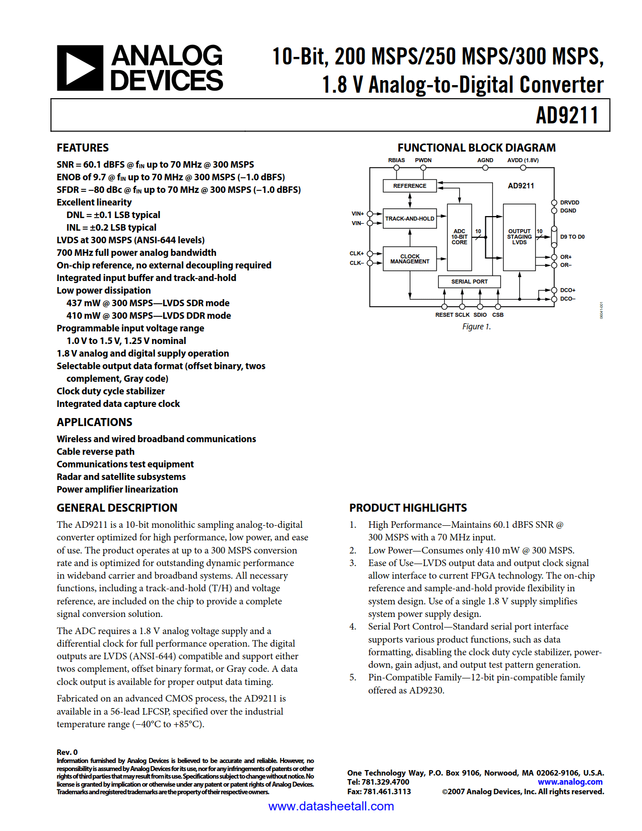
The AD9211 is a 10-bit monolithic sampling analog-to-digital converter optimized for high performance, low power, and ease of use. The product operates at up to a 300 MSPS conversion rate and is optimized for outstanding dynamic performance in wideband carrier and broadband systems. All necessary functions, including a track-and-hold (T/H) and voltage reference, are included on the chip to provide a complete signal conversion solution.
The ADC requires a 1.8 V analog voltage supply and a differential clock for full performance operation. The digital outputs are LVDS (ANSI-644) compatible and support either twos complement, offset binary format, or Gray code. A data clock output is available for proper output data timing.
Fabricated on an advanced CMOS process, the AD9211 is available in a 56-lead LFCSP, specified over the industrial temperature range (−40°C to +85°C).