AD8600 Datasheet
16-Channel, 8-Bit Multiplying DAC
16-Channel, 8-Bit Multiplying DAC
| Part No. | In Stock | Price | Packaging | SPQ | Marking | MSL | Pins | Temp Range | Package Description |
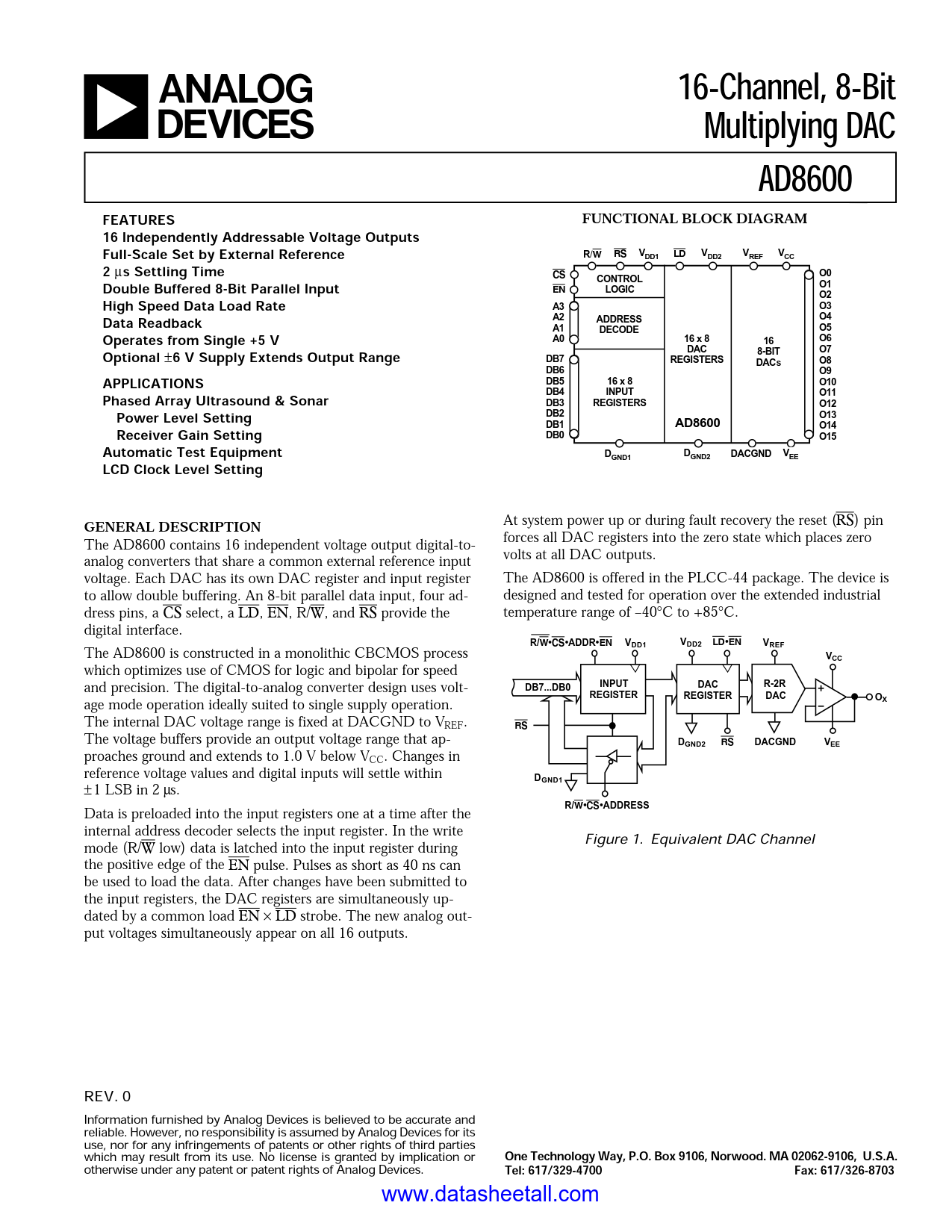
The AD8600 contains 16 independent voltage output digital-to-analog converters that share a common external reference input voltage. Each DAC has its own DAC register and input register to allow double buffering. An 8-bit parallel data input, four address pins, a CS select, a LD, EN, R/W, and RS provide the digital interface.
The AD8600 is constructed in a monolithic CBCMOS process which optimizes use of CMOS for logic and bipolar for speed and precision. The digital-to-analog converter design uses voltage mode operation ideally suited to single supply operation. The internal DAC voltage range is fixed at DACGND to VREF. The voltage buffers provide an output voltage range that approaches ground and extends to 1.0 V below VCC. Changes in reference voltage values and digital inputs will settle within ±1 LSB in 2µs.
Data is preloaded into the input registers one at a time after the internal address decoder selects the input register. In the write mode (R/W low) data is latched into the input register during the positive edge of the EN pulse. Pulses as short as 40 ns can be used to load the data. After changes have been submitted to the input registers, the DAC registers are simultaneously updated by a common load EN x LD strobe. The new analog output voltages simultaneously appear on all 16 outputs.
At system power up or during fault recovery the reset (RS) pin forces all DAC registers into the zero state which places zero volts at all DAC outputs.
The AD8600 is offered in the PLCC-44 package. The device is designed and tested for operation over the extended industrial temperature range of -40°C to +85°C.