AD8311 Datasheet
50 dB GSM PA Controller
50 dB GSM PA Controller
| Part No. | In Stock | Price | Packaging | SPQ | Marking | MSL | Pins | Temp Range | Package Description |
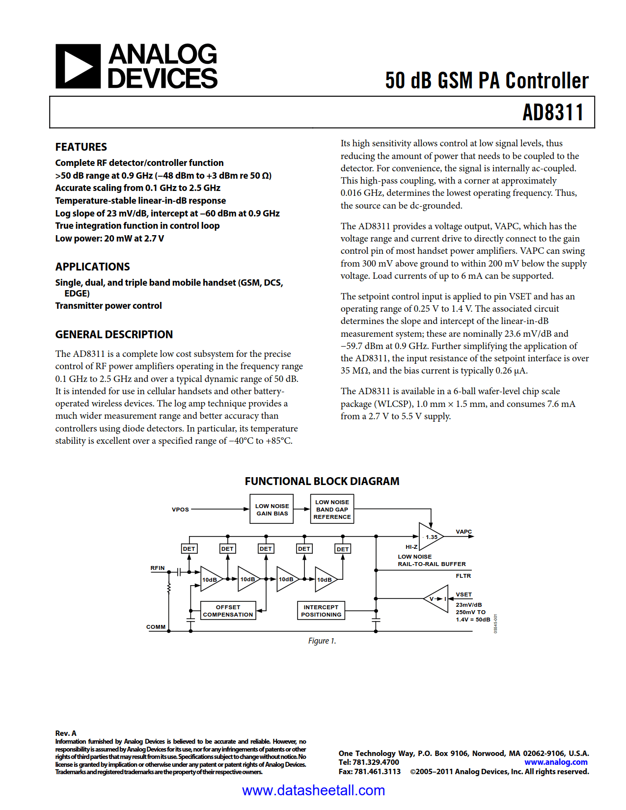
The AD8311 is a complete low cost subsystem for the precise control of RF power amplifiers operating in the frequency range 0.1 GHz to 2.5 GHz and over a typical dynamic range of 50 dB. It is intended for use in cellular handsets and other battery-operated wireless devices. The log amp technique provides a much wider measurement range and better accuracy than controllers using diode detectors. In particular, its temperature stability is excellent over a specified range of −40°C to +85°C.
Its high sensitivity allows control at low signal levels, thus reducing the amount of power that needs to be coupled to the detector. For convenience, the signal is internally ac-coupled. This high-pass coupling, with a corner at approximately 0.016 GHz, determines the lowest operating frequency. Thus, the source can be dc-grounded.
The AD8311 provides a voltage output, VAPC, which has the voltage range and current drive to directly connect to the gain control pin of most handset power amplifiers. VAPC can swing from 300 mV above ground to within 200 mV below the supply voltage. Load currents of up to 6 mA can be supported.
The setpoint control input is applied to pin VSET and has an operating range of 0.25 V to 1.4 V. The associated circuit determines the slope and intercept of the linear-in-dB measurement system; these are nominally 23.6 mV/dB and −59.7 dBm at 0.9 GHz. Further simplifying the application of the AD8311, the input resistance of the setpoint interface is over 35 MΩ, and the bias current is typically 0.26 μA.
The AD8311 is available in a 6-ball wafer-level chip scale package (WLCSP), 1.0 mm × 1.5 mm, and consumes 7.6 mA from a 2.7 V to 5.5 V supply.