AD5689R Datasheet

Dual, 16-Bit nanoDAC+ with 2 ppm/°C Reference, SPI Interface

Part No.:
AD5689R
Manufacturer:
Analog Devices, Inc.
Page:
28 Pages
Size:
1019 KB
Views:
0
Update Time:
2026-01-26 10:57:37

AD5689R DataSheet Applicable Part

Part No. In Stock Price Packaging SPQ Marking MSL Pins Temp Range Package Description
SPQ:Standard Pack Quantity;MSL:Moisture Sensitivity Level

AD5689R DataSheet PDF

AD5689R Features

  • High relative accuracy (INL): ±2 LSB maximum at 16 bits 
  • Low drift 2.5 V reference: 2 ppm/°C typical
  • Tiny package: 3 mm × 3 mm, 16-lead LFCSP
  • TUE: ±0.1% of FSR maximum 
  • Offset error: ±1.5 mV maximum
  • Gain error: ±0.1% of FSR maximum
  • High drive capability: 20 mA, 0.5 V from supply rails 
  • User-selectable gain of 1 or 2 (GAIN pin) 
  • Reset to zero scale or midscale (RSTSEL pin)
  • 1.8 V logic compatibility
  • 50 MHz SPI with readback or daisy chain
  • Low glitch: 0.5 nV-sec
  • Low power: 3.3 mW at 3 V 
  • 2.7 V to 5.5 V power supply
  • −40°C to +105°C temperature range
  • AEC-Q100 qualified for automotive applications

AD5689R Applications

  • Optical transceivers
  • Base station power amplifiers
  • Process control (PLC I/O cards)
  • Industrial automation
  • Data acquisition systems

AD5689R Description

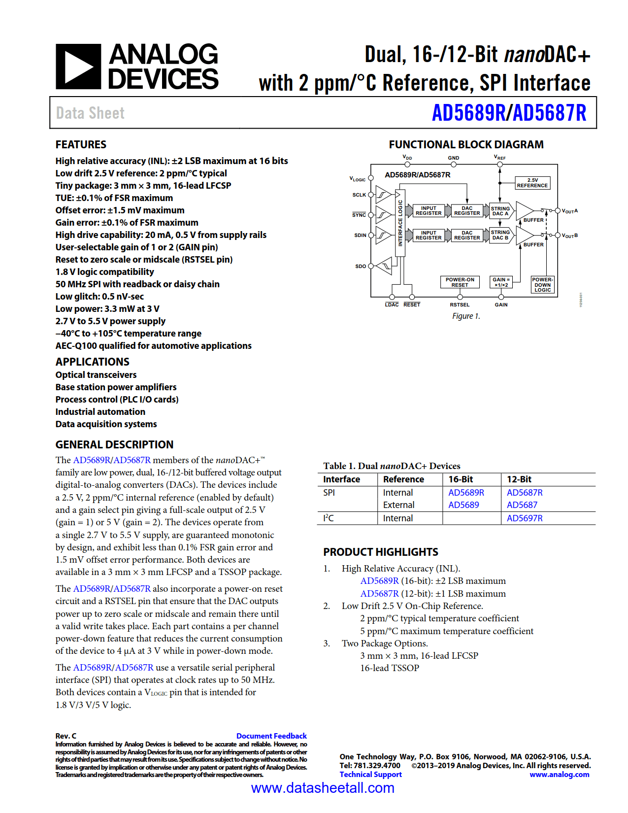
The AD5689R members of the nanoDAC+™ family are low power, dual, 16-bit buffered voltage output digital-to-analog converters (DACs). The devices include a 2.5 V, 2 ppm/°C internal reference (enabled by default) and a gain select pin giving a full-scale output of 2.5 V (gain = 1) or 5 V (gain = 2). The devices operate from a single 2.7 V to 5.5 V supply, are guaranteed monotonic by design, and exhibit less than 0.1% FSR gain error and 1.5 mV offset error performance. Both devices are available in a 3 mm × 3 mm LFCSP and a TSSOP package.

The AD5689R also incorporate a power-on reset circuit and a RSTSEL pin that ensure that the DAC outputs power up to zero scale or midscale and remain there until a valid write takes place. Each part contains a per channel power-down feature that reduces the current consumption of the device to 4 μA at 3 V while in power-down mode.

The AD5689R use a versatile serial peripheral interface (SPI) that operates at clock rates up to 50 MHz. Both devices contain a VLOGIC pin that is intended for 1.8 V/3 V/5 V logic.

PRODUCT HIGHLIGHTS

  1. High Relative Accuracy (INL).
    AD5689R (16-bit): ±2 LSB maximum
  2. Low Drift 2.5 V On-Chip Reference.
    2 ppm/°C typical temperature coefficient
    5 ppm/°C maximum temperature coefficient 
  3. Two Package Options.
    3 mm × 3 mm, 16-lead LFCSP
    16-lead TSSOP

AD5689R Datasheet FAQs