AD5324-EP Datasheet
2.5 V to 5.5 V, 500 μA, Quad Voltage Output 12-Bit DAC in 10-Lead Package
2.5 V to 5.5 V, 500 μA, Quad Voltage Output 12-Bit DAC in 10-Lead Package
| Part No. | In Stock | Price | Packaging | SPQ | Marking | MSL | Pins | Temp Range | Package Description |
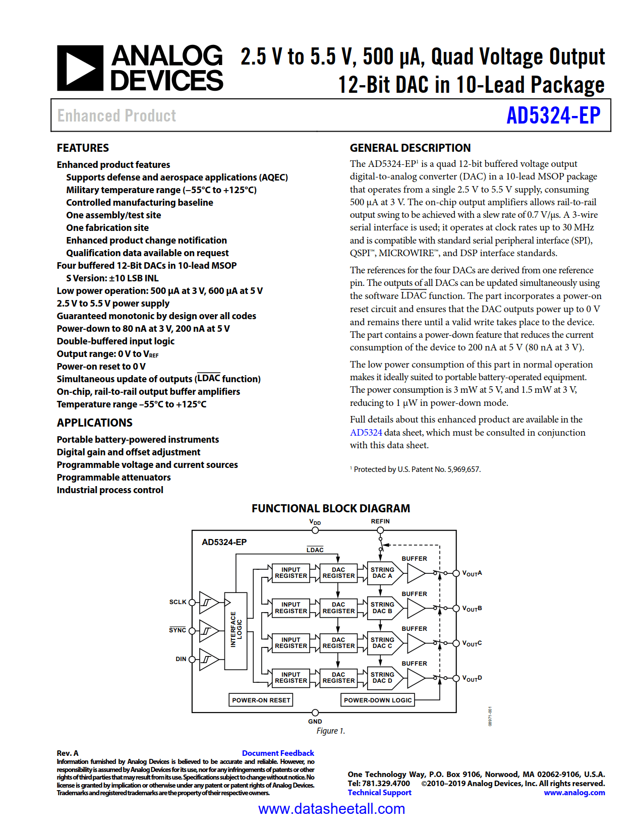
The AD5324-EP is a quad 12-bit buffered voltage output digital-to-analog converter (DAC) in a 10-lead MSOP package that operates from a single 2.5 V to 5.5 V supply, consuming 500 μA at 3 V. The on-chip output amplifiers allows rail-to-rail output swing to be achieved with a slew rate of 0.7 V/μs. A 3-wire serial interface is used; it operates at clock rates up to 30 MHz and is compatible with standard serial peripheral interface (SPI), QSPI™, MICROWIRE™, and DSP interface standards.
The references for the four DACs are derived from one reference pin. The outputs of all DACs can be updated simultaneously using the software LDAC function. The part incorporates a power-on reset circuit and ensures that the DAC outputs power up to 0 V and remains there until a valid write takes place to the device. The part contains a power-down feature that reduces the current consumption of the device to 200 nA at 5 V (80 nA at 3 V).
The low power consumption of this part in normal operation makes it ideally suited to portable battery-operated equipment. The power consumption is 3 mW at 5 V, and 1.5 mW at 3 V, reducing to 1 μW in power-down mode.
Full details about this enhanced product are available in the AD5324 data sheet, which must be consulted in conjunction with this data sheet.