AD5322 Datasheet
2.5 V to 5.5 V, 230 µA, Dual Rail-to-Rail Voltage Output 12-Bit DAC
2.5 V to 5.5 V, 230 µA, Dual Rail-to-Rail Voltage Output 12-Bit DAC
| Part No. | In Stock | Price | Packaging | SPQ | Marking | MSL | Pins | Temp Range | Package Description |
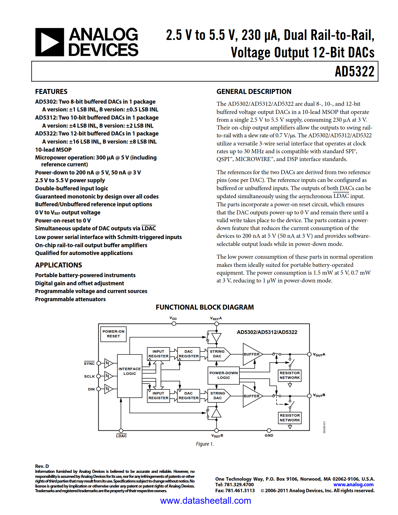
The AD5322 are dual 12-bit buffered voltage output DACs in a 10-lead µSOIC package that operate from a single +2.5 V to +5.5 V supply consuming 230 µA at 3 V. Their on-chip output amplifiers allow the outputs to swing rail-to-rail with a slew rate of 0.7 V/µs. The AD5322 utilize a versatile 3-wire serial interface which operates at clock rates up to 30 MHz and is compatible with standard SPI™, QSPI™, MICROWIRE™ and DSP interface standards.
The references for the two DACs are derived from two reference pins (one per DAC). The reference inputs can be configured as buffered or unbuffered inputs. The outputs of both DACs can be updated simultaneously using the asynchronous LDAC input. The parts incorporate a power-on reset circuit, which ensures that the DAC outputs power-up to 0 V and remain there until a valid write takes place to the device. The parts contain a power-down feature that reduces the current consumption of the devices to 200 nA at 5 V (50 nA at 3 V) and provides software-selectable output loads while in power-down mode.
The low power consumption of these parts in normal operation makes them ideally suited for portable battery-operated equipment. The power consumption is 1.5 mW at 5 V, 0.7 mW at 3 V, reducing to 1 μW in power-down mode.