AD1671 Datasheet
Complete 12-Bit 1.25 MSPS Monolithic A/D Converter
Complete 12-Bit 1.25 MSPS Monolithic A/D Converter
| Part No. | In Stock | Price | Packaging | SPQ | Marking | MSL | Pins | Temp Range | Package Description |
The AD1671 is a monolithic 12-bit, 1.25 MSPS analog-to-digital converter with an on-board, high performance sample-and-hold amplifier (SHA) and voltage reference. The AD1671 guarantees no missing codes over the full operating temperature range. The combination of a merged high speed bipolar/ CMOS process and a novel architecture results in a combination of speed and power consumption far superior to previously available hybrid implementations. Additionally, the greater reliability of monolithic construction offers improved system reliability and lower costs than hybrid designs.
The fast settling input SHA is equally suited for both multiplexed systems that switch negative to positive full-scale voltage levels in successive channels and sampling inputs at frequencies up to and beyond the Nyquist rate. The AD1671 provides both reference output and reference input pins, allowing the on-board reference to serve as a system reference. An external reference can also be chosen to suit the dc accuracy and temperature drift requirements of the application.
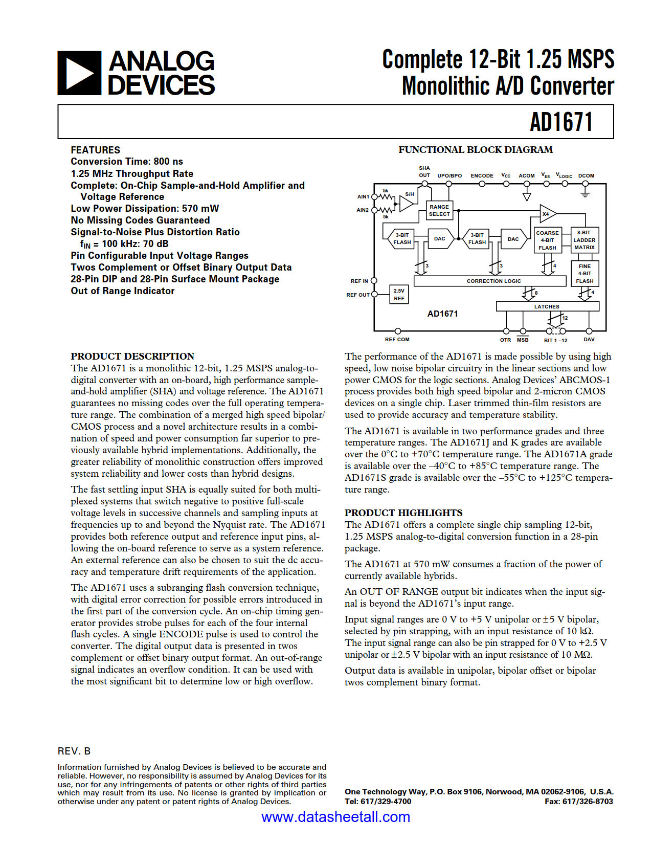
The AD1671 uses a subranging flash conversion technique, with digital error correction for possible errors introduced in the first part of the conversion cycle. An on-chip timing generator provides strobe pulses for each of the four internal flash cycles. A single ENCODE pulse is used to control the converter. The digital output data is presented in twos complement or offset binary output format. An out-of-range signal indicates an overflow condition. It can be used with the most significant bit to determine low or high overflow.
The performance of the AD1671 is made possible by using high speed, low noise bipolar circuitry in the linear sections and low power CMOS for the logic sections. Analog Devices' ABCMOS-1 process provides both high speed bipolar and 2-micron CMOS devices on a single chip. Laser trimmed thin-film resistors are used to provide accuracy and temperature stability.
The AD1671 is available in two performance grades and three temperature ranges. The AD1671J and K grades are available over the 0°C to +70°C temperature range. The AD1671A grade is available over the -40°C to +85°C temperature range. The AD1671S grade is available over the -55°C to +125°C temperature range.